


Enhanced Surface Potential Detection Study using FM-KPFM
John Paul Pineda, Charles Kim,Cathy Lee, Byong Kim, and Keibock Lee Park Systems Inc., Santa Clara, CA USA
Introduction
Scanning Kelvin probe microscopy (KPFM) is a tool used to measure work function and local electrical potential distribution of various materials with nanoscale features. The most common application of this technique is the study of electronic properties of semiconductor nanostructures and surfaces. Potential profiling of such materials composing of negatively or positively charged substancesis some of the measurements can be done using this technique with nanoscale lateral resolution. Implementation of such techniqueto unveiling thevariations of charge distribution that occurs on the nanoscale can help better understanding and improving the performance of CMOS semiconductor devices.[1-2] Such KPFM has also been instrumental incharacterizing and determining the quantitative physical information such as the total charge and charge position of polymer materials.[3, 4] There are other surface potential or work function measuring tool that were introduced such as electron beam induced current (EBIC), scanning electron microscopy (SEM), and photoelectron spectroscopy (PES). However, some of these techniques are only applicable for inorganic type semiconductor samples, some are destructive and requires high vacuum, and others do not provide high spatial resolution.[5] Compared to other techniques, KPFM is nondestructive and air-ambient compatible technique which unequivocally is one of the most easy to use electrical failure analysis and nanometrology tool available in the market today. Conventional KPFM technique (also known as Amplitude Modulation AM-KPFM) has alreadymade remarkable contribution in maintaining device reliability and analysis of advance materials compared to other measurement techniques, but there is room for improvement in the signal to noisedetection ability of AM-KPFM technique so that even the featureshaving less optimal surface potential strength can be detectedand mapped out with higher lateralresolution and accuracy. Toward this end, recently, Park Systems developed a technique called Frequency Modulation FM-KPFM with Atomic Force Microscope (AFM). This technique is useful for electrical characterization allowing measurements with better sensitivity compared to AM-KPFM.In this study, a polymer material was measured to compare the performance of AM-KPFM to FM-KPFM. The results acquired in the experiment show that FM-KPFM is significantlymore sensitive compared to AM-KPFM in measuring both work function and surface potential distribution of different materials.
Experimental
A polymer patterned array material deposited on Silicon substrate was analyzed using a Park NX10 AFM. Two separate scans were conducted to acquire AM-KPFM and FM-KPFM measurements. The scan parameters and the tip used in acquiring images were all the same. A conductive Mikromasch NSC36Cr-Au cantilever (nominal spring constant k = 1 N/m with resonant frequency f = 90 kHz) was used in the experiment. In KPFM mode, there are two interaction forces between the AC biased tip and the sample: the electrostatic force and Van der Waals force. The Van der Waals force is harnessed to generate the sample's surface topography while the electrostatic force between the tip and sample generates data for the sample's electrical properties. The obtained cantilever deflection signal contains both sets of information; therefore, a method that can completely separate these signals is the key to successful imaging. In the Park NX10, lock-in amplifiers embedded to its electronics are used to separate the signals. This allows for the acquisition of both topography and EFM data simultaneously. Two amplifiers are used by the system, named lock-in 1 and lock-in 2. Lock-in 1 obtains the topography information by analyzing the tip motion caused by the Van der Waals interaction, while lock-in 2 obtains electrical property information by analyzing the frequency of the applied AC voltage signal to the tip which, in turn, generates an electrostatic force interaction with the sample. The frequency of the applied AC voltage signal is chosen to be smaller (5 - 20 kHz) than the cantilever oscillation frequency (70- 330 kHz), enough so that the two signals do not interfere each other. In FM-KPFM setup [6], the NCM phase signal of Lock-in 1 is transferred to Lock-in 2 to serve as a source for EFM operation by connecting BNC cable between ‘Aux2 out’ and ‘Aux1 in’ shown in Figure 1. Furthermore, a separate DC bias was applied to the cantilever and controlled for to create a feedback loop that would zero out the electrical oscillation between the tip and the sample caused by the application of an AC bias to the cantilever. The value of this offsetting DC bias that zeroes out the AC bias-induced electrical oscillation is considered to be a measure of surface potential.
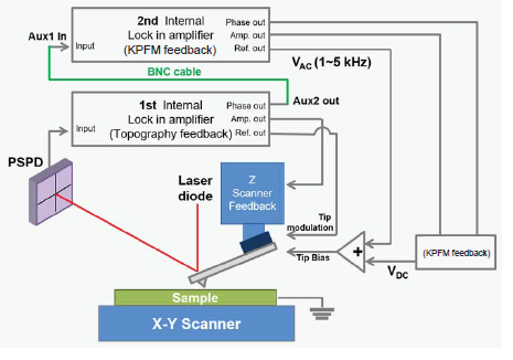
Fig. 1. Diagram of FM-KPFM
Results and Discussion
The topography data obtained in this experiment shows that polymer patterned array with square-like features were successfully deposited on silicon substrate and no significant information related to its surface potential was provided. In contrast, the surface potential data acquired in AM-KPFM and FM-KPFM shows the surface potential structure, but no significant information related to physical structure of the sample. The domain structure shape observed in KPFM data of the sample was similar to the physical structure observed in topography data, which was a patterned array consisting of square dots. The data acquired in this experiment were all analyzed using Park XEI software developed by Park Systems. Figure 2 shows the topography (left), FM-KPFM (center), and AM-KPFM (right) images of the polymer patterned array sample. The topography data can be acquired simultaneously with the KPFM data. In Figure 2, the topography image presented was acquired simultaneously with the AM-KPFM image. The topography shows a clear image of a well-defined lattice structure. The Park XEI software maps the acquired signals into a color table. In the topography image, the square-like features which appeared to have a brighter color represent the areas with higher height while the flat surface with darker color represents the areas with lower height. The measured peak to valley in the topography image was approximately 150 nm. On the other hand, both AM-KPFM and FM-KPFM data show a patterned array with an irregularity on the surface (pointed by red arrows). In the two KPFM images, the square-like features which appear to have a darker color, represent the areas with relatively lower surface potential while the flat surface with brighter color represent the areas with higher surface potential. By comparing the surface potential results acquired from AM-KPFM and FM-KPFM, one can easily determine that FM-KPFM has better sensitivity in detecting surface potential variation compared to AM-KPFM. In this experiment, FM-KPFM technique provided a higher resolution image that shows sharper edges of the square features compared to AM-KPFM. In addition, FM-KPFM was able to detect weak potential in the irregular surface while AM-KPFM was not able to detect any potential variation.
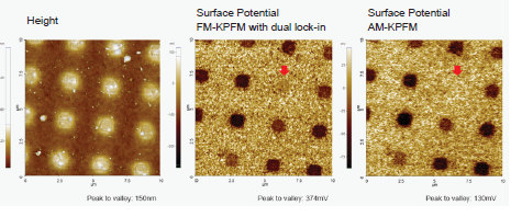
Fig. 2. 10x10 μm image of polymer patterned array. Topography image (left), FM-KPFM image (center),
and AM-KPFM image (right).
The line profile that was generated by the XEI software in Figure 3 (bottom) provides the potential information of the polymer patterned array. The line profile for the FM-KPFM is indicated in color red while the line profile for AM-KPFM is indicated in color green. The line profile of the FM-KPFM image clearly shows that there is a slightly decreasein potential (encircled in red) in the irregular surface compared to the areas next to it. On the other, the line profile of AM-KPFM doesn’t show any changes of potential in that surface. By comparing the line profile of the two techniques, it can be concluded that FM-KPFM is at least an order of magnitude more sensitive than conventional AM-KPFM technique.
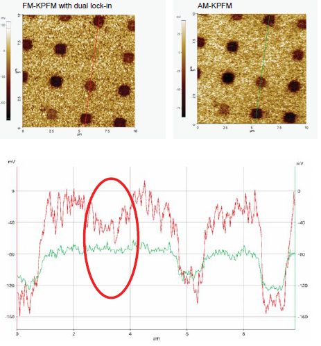
Fig. 3. FM-KPFM image (top-left), AM-KPFM image (top-right) and corresponding line profile (bottom) acquired from the polymer sample. FM-KPFM line profile (red line, y-axis on left) and AM-KPFM line profile (green, y-axis on right).
Conclusion
The polymer patterned array was successfully characterized by the Park NX10 AFM using AM and FM-KPFM imaging. The topography data revealed that the sample surface is composed of patterned array with square-like features. An irregularity in the patterned array was observed in both AM-KPFM and FM-KPFM images. FM-KPFM technique shows that the irregularity in the surface pattern is a surface with weak potential. AM-KPFM technique was not sensitive enough to detect the weak potential in the same region. Given the above results, it can be concluded that FM-KPFM is an order of magnitude more sensitive compared to AM-KPFM and it is more useful in detecting surface potential variations. The increased in sensitivity of this technique will also increase the chance of detecting defects with improved resolution and accuracy in semiconductor devices and other advanced materials.
References
1. LanFei (2018) FUNDAMENTALS OF KELVIN PROBE FORCE MICROSCOPY AND ITS APPLICATIONS IN THE CHARACTERIZATION OF SOLAR CELLS. Doctoral Dissertation, University of Pittsburgh.
2. J.Pineda, et al., Electrical Characterization of Semiconductor Device Using SCM and KPFM Imaging.terization.
3. J. Gonzalez, et al., Charge distribution from KPFM images, PCCP, Issue 40, 2017.
4. M. Ortuño, et al., Conducting polymers as electron glasses: surface charge domains and slow relaxation, Scientific Reports volume 6, Article number: 21647 (2016).
5. W. Melitz, et al., Kelvin probe force microscopy and its application, Surface Science Reports 66 (2011) 1–27.
6. Charles Kim, et al., How to Measure FM-KPFM, Park Systems White Paper, To be published (2018)