


The Latest Advances in AFM Metrology for Nanofabrication at imec
Come join us from 10:00 to 11:30 AM at the State University of New York (SUNY) Polytechnic Institute on Friday, May 19 we serve up some breakfast goodies and friendly discourse as we all catch up on our work at the nanoscale with atomic force microscopy (AFM)!
SUNY Polytechnic Institute
NanoFab South Building
255 Fuller Road
Albany, NY 12203
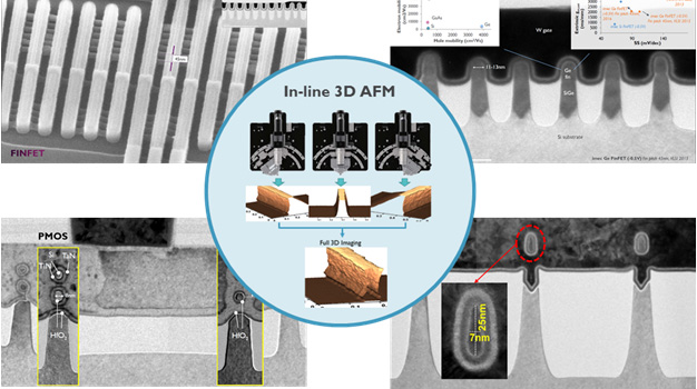
This month, join us as we welcome a special guest speaker, imec Senior Researcher, Dr. Tae-Gon Kim! Dr. Kim will be on hand to discuss the advances that have been made with AFM-based 3D metrology. His talk, titled "In-line (3D) AFM as Solution Provider for Beyond N10 Process" as well as a complementary talk from our own staff in attendance on “Automated AFM for Small-Scale and Large-Scale Surface Profiling in CMP Applications” will be the featured items on event program.
Learn more our speakers below:

Dr. Tae-Gon Kim
Senior Researcher at imec
In-line (3D) AFM as Solution Provider for Beyond N10 Process
Atomic force microscopy (AFM) was introduced 30 years ago and it has been widely used in various technology domains such as material science, semiconductor, biotechnology, and so on in order to understand mechanical and chemical properties of materials fundamentally as well as the physical and chemical interactions between materials at nanoscale. Even though this technique contributes to technological improvements, AFM is one of the techniques that does not seem to be considered a metrology tool for high volume manufacturing. It may be caused by low productivity due to long measurement lead time and less user-friendliness as compared to other high-throughput metrology techniques such as CD-SEM and scatterometry (or OCD) and so on. As structure size is getting smaller and smaller, atomic resolution and gage R&R of sub-atomic levels without structure is required in metrology. The issue becomes especially critical in the semiconductor industry because devices scale down to 10, 7, and 5 nm. Furthemore, device shape becomes vertical and three-dimensional as with a horizontal or vertical nanowire. Semiconductor industry demands metrology techniques to fulfill these types of requirements.
In this presentation, what solutions in-line (3D) AFM can provide at different processes such as etch, CMP, lithography, and device applications (FinFET and 3D packaging) are discussed. It also shows what AFM activities at imec are done in order to fulfill the needs of the semiconductor industry in terms of production compatibility.
About Dr. Tae-Gon Kim
Tae-Gon Kim received his masters degree in materials science and engineering in 2001 and his PhD degree in 2008 from Hanyang University in South Korea. Since 2010, he is a scientific researcher responsible for in-line metrology at imec Belgium. In his reserach career, he has been leading activity on advanced film characterization as well as in-line metrology techniques for STT-MRAM devices and in-line 3D-AFM technology for 3 dimensional structure characterization such as sidewall characterization of FinFET and nanowires. He developed a new methodology of measuring pattern strength and particle adhesion forces using atomic force microscope and reported the world's first physical cleaning process window as a result of the study. He has been a postdoctoral research fellow at KU Leuven (2008-2010) and in 2010 he became a senior researcher at imec. He contributes to academia as an adjunct professor at Hanyang University.
Dr. Ardavan Zandiatashbar
Technical Accounts Manager at Park Systems
Automated AFM for Small-Scale and Large-Scale Surface Profiling in CMP Applications
As the feature size is shrinking in the foundries, the need for inline high resolution surface profiling with versatile capabilities is increasing. One of the important areas of this need is chemical mechanical planarization (CMP) process. We introduce a new generation of atomic force profiler (AFP) using decoupled scanners design. The system is capable of providing small-scale profiling using XY scanner and large-scale profiling using the slider. Decoupled scanners design enables enhanced vision which helps minimizing the positioning error for locations of interest in case of highly polished dies. Non-Contact mode imaging is another feature of interest in this system which is used for surface roughness measurement, automatic defect review, and deep trench measurement. Examples of the measurements performed using the atomic force profiler is demonstrated.