


Detect the defect - Advantages of Automated Atomic Force Microscopy [AFM] for Semiconductor Applications
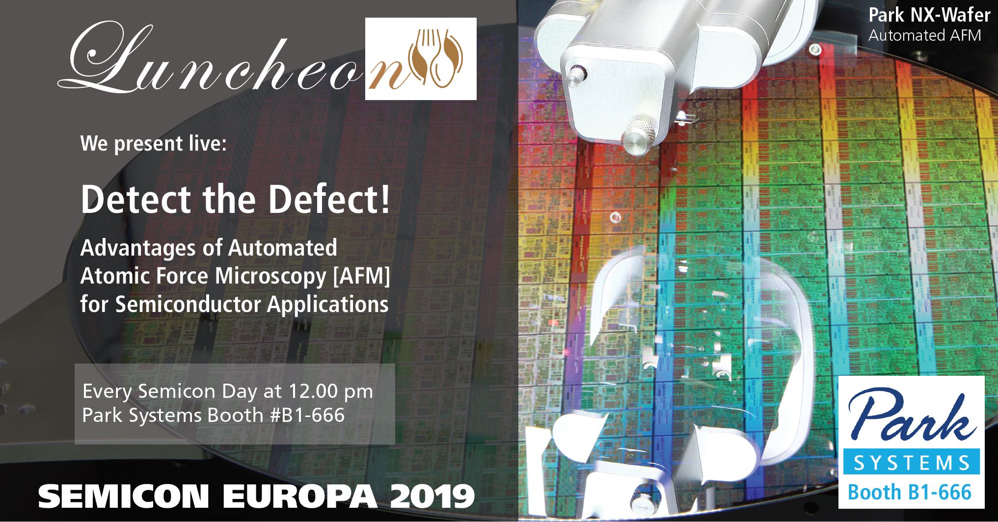
Detect the Defect! Advantages of Automated Atomic Force Microscopy [AFM] for Semiconductor Applications
We are delighted to invite you to join our LUNCHEONS on every SEMICON EUROPA day at 12:00 pm, Park Systems Booth B1-666.
Enjoy the lunch snacks and the seminar on: “Detect the defect! - on Advantages of Automated Atomic Force Microscopy [AFM] for Semiconductor Applications,” presented by Dr. Christian Froeck.
In the 30-minutes presentation we will be revealing the latest insights into AFM industrial applications such as Automatic Defect Review, 3D surface information, surface roughness, trench depth, via or bump analysis, High Vacuum AFM for Electrical Measurements and Failure Analysis, and more!
Date: Tuesday, November 12 – Friday, November 15, 2019
Time: 12:00 pm
Place: Neue Messe München, Munich, Germany
The LUNCHEON is open to everyone and is FREE of charge.
Registration and contact: pse@parksystems.com | www.parksystems.com
ABSTRACT
Surface investigation is useful to improve yield and quality of semiconductor products. In particular, the detection and characterization of defects play an important role for optimizing production processes. Automatic Defect Review Atomic Force Microscope (ADR AFM) from Park Systems is a tool for inline or offline wafer inspection to generate three dimensional (3D) images of defects.
Conventional optical instruments, like Automated Optical Inspection (AOI) systems, allow a higher throughput but cannot provide the resolution, which is necessary for the inspection of today’s semiconductor structures. Since AOI is restricted by the diffraction limit, ADR AFM complements it by capability of characterizing features in the range of several nanometers.
Furthermore, the ADR AFM provides 3D information of defects which cannot be given by optical or other methods like SEM. The True Non-ContactTM measuring mode, available on Park’s ADR AFM, enables the non-destructive surface characterization of the semiconductor (contrary to SEM) ensuring the long tip lifetime without the necessity of exchanging the probe. In addition to the defect review capabilities, the ADR AFM from Park Systems functions as a conventional AFM to obtain 3D information of semiconductor structures. Surface roughness, trench depth, via or bump analysis can be measured inline during the production, or offline in a metrology laboratory. The data received can be used to optimize production processes and to qualify process steps.
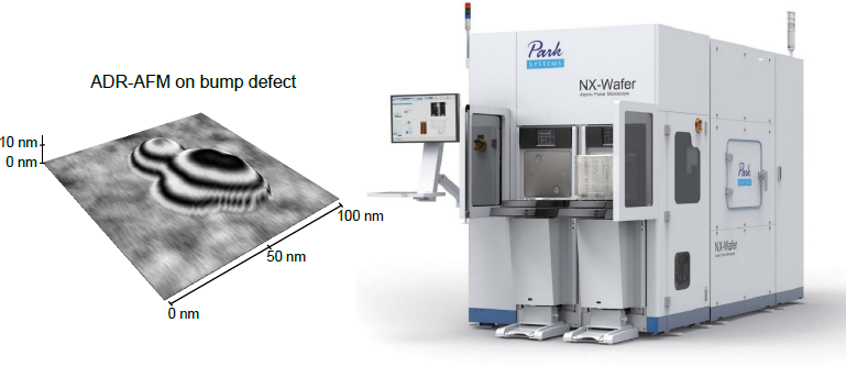
NX-Wafer
About SEMICON EUROPA
The Semicon Europa is Europe's leading showcase for technologies that are at the cutting edge of the microelectronics industry and highlights the areas of research and development. As an information and communication platform it offers high-caliber technical conferences, forums and programs and excellent networking opportunities. Please visit http://www.semiconeuropa.org/ for more information.