


HOSSEIN ROKNI DAMAVANDI TAHER
Hossein Rokni Damavandi Taher is currently a Postdoctoral Research Fellow in Prof. Wei Lu’s group at the University of Michigan. He earned his Ph.D. from University of Michigan in 2018, M.S. from University of British Columbia in 2011 and B.S. from Iran University of Science and Technology in 2005, all in Mechanical Engineering. He is the recipient of the 2015 I.K. McIvor Award for excellence in research and scholarship in Applied Mechanics and the 2016 Rackham Predoctoral Fellowship Award for unusually creative, ambitious and impactful dissertation research and the nominee for the 2018 ProQuest Distinguished Dissertation Award. He has also co-authored over 50 publications with more than 1100 citations. His research focuses on micro/nanomechanics, micro/ nanocharacterization and atomistic-tocontinuum modeling of atomically thin layered materials, vdWhetero structures, biomaterials and smart materials as well as on the development of MEMS/NEMS devices incorporating such materials.
Please summarize the research you do and explain why it is significant?
My current research mainly focuses on developingnovel micro/nanoscale measurement techniques combined with multiscale modeling at the atomistic and continuum levels to advance our fundamental understanding of mechanical and electrical behavior of atomically thin layered materials and newly emerged vdWhetero structures. Such powerful characterization techniques are then to be leveraged to improve synthesis, transfer, manipulation, integration and performance of opto-, bio- and nanoelectronic devices incorporating 2D layered materials and vdWheterostructures.
How might your research be used?
Atomically thin layered materials (ATLMs), such as graphene, hexagonal boron nitride and transition metal dichalcogenides (e.g., MoS2 and WS2),and vdWheterostructures have catapulted nanoscience and nanotechnology to unimaginable new heights in a relatively short period of time since graphene was isolated from bulk graphite in 2004. They exhibit a unique combination of high elasticity, extreme mechanical flexibility, visual transparency, and superior electronic performancethat are not essentially observed in their bulk crystals, making them ideally suited to modern devices, such as flexible biosensors, photovoltaic devices, fast charging lithium ion batteries, transparent touchscreen displays, hydrogen evolution catalysis, flexible transistors, photo detectors, and memory devices. However, scalable, controllable and cost-effective production of ATLMs with high quality has still remained challenging mainly due to the poor understanding of the nature of weak interlayer interactions and the lack of precise experimental techniques to characterize such complex interlayer behavior of ATLMs. As a means to address such a challenging issue, we combined conductive atomic force microscopy and molecular dynamics simulations to unravel the relative contributions of electrostatic attraction/ repulsion interactions and highly anisotropic vdW interactions to the exfoliation of the ATLMs from their bulk crystals. This unique nanoscale manipulation setup also allowed us not only to quantify, for the first time, the effect of layer number and electric field on the dielectric constant of ATLMs with few-layer down to monolayer thickness, but also to successfully produce The University of Michigan’s thinnest possible logo by only mono-, bi- and trilayer graphene flakes, thanks to the ultrahigh forcedisplacement resolution of the conductive AFMassisted electrostatic manipulation setup.
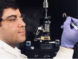
Why is the Park AFM important for your research?
The nature of our research requires a unique combination of high-resolution imaging, nanoscale mechanical manipulation and precise in-situ measurements of atomically thin layered materials (ATLMs) and newly emerged van der Waals (vdW) heterostructures. Fortunately, our Park XE-70 atomic force microscope offers such a unique nanoscale manipulation setup with ultra high forcedisplacement resolution, making nanoscale probing of weak interlayer interactions in ATLMs and vdWhetero structures possible.
What features of Park AFM are the most beneficial and why?
The novel design of the Park XE-70 AFM coupled with highly user-friendly interface software XEP has made it possible to simultaneously image sample surfaces with atomic-scale resolution, precisely manipulate nano-objects down to single molecules and accurately measure the physical properties of interest through a comprehensive range of innovative modes supported by the Park AFM (e.g., imaging mode, electrical mode,nanomechanical mode, etc.). Also, data analysis software XEI, which is widely used in our lab for the physical and structural characterization of nano-features, plays a crucial role in extracting the essential information from our AFM measurements.