


JAMEY GIGLIOTTI
PHD CANDIDATE GEORGIA INSTITUTE OF TECHNOLOGY, SCHOOL OF MATERIALS SCIENCE AND ENGINEERING
Jamey Gigliotti is a PhD candidate at the Georgia Institute of Technology in the School of Materials Science and Engineering. He began his tenure at Georgia Tech studying the growth of nanoscale piezoelectric films before joining the Epitaxial Graphene Lab where he continues to work in close collaboration with researchers at Georgia Tech Lorraine in Metz, France. Before coming to Georgia Tech, Jamey completed his undergraduate education at Penn State University, a few hours from his hometown of Harrisburg, Pa. While at Penn State, he worked on piezoelectric micromachined ultrasonic transducers for medical imaging and sonotweezing applications. This research took him to Germany to work with ultrasound simulation experts. While the focus of his research has changed several times, a unifying theme has been the deposition and characterization of nanoscale material systems. He plans to continue along this theme, but with a new focus after graduation.
1. Summarize the research you are doing and explain briefly how it will impact society. Why is your research important?
Nanoelectronics are a pervasive technology, but have not undergone a transformative technology change in decades. Epitaxial graphene, a single layer of carbon atoms arranged in a honeycomb lattice on a single crystal SiC substrate, is a promising technology platform to disrupt the silicon industry due to its unique electronic transport and robust thermal and chemical stability. However, despite billions of dollars in research, graphene technology has not trickled into industrial products, largely due to the need to reliably integrate graphene with dielectric and semiconducting materials to make useful and reliable electronics. Boron nitride, a dielectric isomorph to graphene, is an ideal candidate material which has been shown to preserve the electronic transport of graphene. Yet, to date, a scalable method to produce grapheneBN heterostructures has not been found. My research focuses on developing novel deposition techniques to enable epitaxial growth of boron nitride layers directly on pristine graphene surfaces, a necessary step to achieving industrially relevant graphene-based nanoelectronics
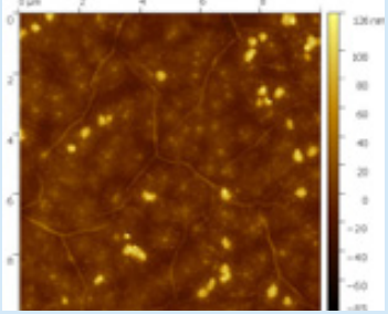
A 20 nm thick boron nitride film deposited on a monolayer of eptiaxial graphene. This topographical AFM image shows the pleated BN surface which is indicative of a 2D layered structures due to the negative in-plane coefficient of thermal expansion.
2. What is the most useful part of using Park AFM for your research? Please explain what features are most useful and why?
Graphene and BN are both 2D materials and demand a unique suite of characterization tools including scanning probe, electron microscopy, diffraction, and optical techniques. Scanning probe techniques are highly sensitive to surface topography and chemical states. As such, the Park AFM provides us with a direct probe of the individual atomic layers and can aid in differentiating SiC, buffer layer, graphene, and boron nitride regions, which is extremely difficult with scanning electron microscopy. For this, lateral force microscopy (LFM) is vitally important and can identify nanoscale regions of graphene and boron nitride from the SiC substrate. Graphene and boron nitride, both sp2 bonded materials, interact only very weakly with the tip compared to SiC, which provides a stark imaging contrast. This information aids in our understanding of how these domains nucleate and grow, which guides the development of our custom deposition tools and processing conditions to achieve higher quality materials with more control over their morphology.