


PinPoint Piezoelectric Force Microscopy
Wenqing Shi, Cathy Lee, Gerald Pascual, John Paul Pineda, Byong Kim, Keibock Lee Park Systems Inc., Santa Clara, CA USA
ABSTRACT
Electromechanical couplingin materials is a key property that provides functionality to a variety of applications,including sensors, actuators, IR detectors, energy harvesting and biology. Most materials exhibit electromechanical coupling in nanometer-sized domains. Therefore, to understand the relationships between structure and function of these materials, characterization at nanoscale is required. This electromechanical coupling property can be directly measured in a non-destructive manner using piezoelectric force microscopy (PFM), a mode that comes standard in all Park atomic force microscopes (AFMs). Here in this application note, we developed a novel technique termed as PinPoint™ PFM and demonstrated the application of PinPoint PFM in the characterization of annealed phenanthrenethin film on top of an ITO surface. The phenanthrenematerial has been a challenging sample to get quality topographical and piezoelectric response data from using conventional SPM methods. The main difficulty is due to the rod-shaped nanostructures on the sample surface being very susceptible to displacement by a scanning probe's tip. The invention of Park's latest PinPoint PFM technique gives researchers both a friction-less imaging technology that overcomes this difficulty and the means to achieve publication-ready image quality in much less time than previously possible with older methods. Here we demonstrated, not only can image well-resolved individual rod-shaped phenanthrene structures, but also differences in electrical polarization expressed as differences in PFM contrast (brighter areas showing a positive polarization and darker areas a negative polarization) without image distortions.
Introduction
Piezoelectric effect, is an intrinsic material property, in which the application of an electric field leads to thickness changes and/or shearing of the material. This unique electromechanical coupling property has been employed in a wide range of applications ranging from medical imaging and energy harvesting, to actuators and sensors.1 Example of piezoelectric materials include crystals (i.e., quartz), biological materials (i.e., DNA, bones and proteins) and man-made materials such as synthetic ceramics (barium titanate and zinc oxide) and some organic thin films.3 Driven by the developing nanotechnology and the increasing demands for miniaturization of electronic devices, characterization of piezoelectric effect at micro- and nanoscale has attracted significant interest. Piezoelectric force microscopy (PFM), also termed as dynamic-contact electrostatic force microscopy (DC-EFM) by Park, is an atomic force microscopy (AFM) based method that allows for high-resolution imaging, quantification and manipulation of piezoelectric materials at micron- and nanometer-length scale. Conventional PFM is usually performed in contact mode, and concurrent topographic imaging and piezoresponse measurements is obtained. In conventional PFM operation, an electrically-biased conductive tip is brought in contact with the surface of a piezoelectric material. Through application of an AC modulation to the conductive tip, the piezoelectric response of the material can then be measured by tracking the deflection of the cantilever as a result of sample’s local expansion or contraction based on the applied electric field. As these surface displacement are often very small with a low signal-to-noise ratio, and, thus, a lock-in amplifier is used for the detection of the amplitude and phase of the piezoelectric response signal. In terms of the AC bias frequency selection, a frequency that’s much lower compared to the cantilever’s resonance frequency is used. In addition, a DC bias can be applied to the sample to switch the domains of the piezoelectric material. Since the atomic force microscopy’s photodiode is position-sensitive, piezoelectric force microscopy can also identify the direction of electrical polarization in piezoelectric or ferroelectric domains. There are two modes of PFM imaging: vertical PFM (VPFM) and lateral PFM (LPFM), which are sensitive to domains polarized out-of-plane and in-plane, respectively.2 (Figure 1) In vertical piezoelectric force microscopy, in the presence of piezoelectric domains that point out-of-plane or perpendicular to the sample surface (Figure 1a-b), the cantilever will deflect vertically with respect to the sample surface in response to the applied electric field. Therefore, the PFM signal will appear bright for domains that point upward and dark for domains that point downward. In lateral piezoelectric force microscopy, in the presence of in-plane piezoelectric domains that’s parallel to the surface, a displacement shearing on the surface will occur. As a result, a torsional displacement of the cantilever will be induced, which in turn will be captured by the position sensitive photo detector as a lateral deflection. (Figure 1c-d)
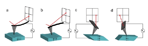
Fig. 1.A schematic representation of (a-b) vertical and (c-d) lateral PFM. The AFM laser shows vertical deflections which correspond with (a) downward or (b) upward out-of-plane electrical polarization. In lateral PFM, the cantilever will exhibit torsion in response to (c-d) lateral in-plane polarization directions. Black arrows indicate the direction of polarization vector in each case assuming that the relationship between polarization and crystal orientation is conserved.
In this application note, piezoelectric force microscopy is performed utilizing the newly-developed PinPoint™ mode by Park Systems as opposed to the conventional contact mode. Performance comparison of PinPoint™ PFM and conventional PFM was carried out on annealed phenanthrene film, and improved resolution was observed in both topography and piezoelectric response signal with PinPoint™ PFM. In PinPoint™ PFM mode, the AFM probe monitors its feedback signal, approaches towardsthe sample surface until a predefined force threshold point is reached, measures the Z scanner’s height, then the AFM probe is rapidly retracted away from the surface to a user-defined height. The XY scanner stops during the piezoelectric response acquisition, and the probe-substrate contact time is controlled to allowsufficient time for quality data acquisition (Figure 2). PinPoint PFM allows higher spatial resolution with optimized piezoelectric response measurement over different sample surface.PinPoint PFM was designed to replace the conventional contact PFM and is an enhanced design that eliminates the problems of the tip wearing out during contact mode topography and diminished contact time. The PinPoint™ PFM technology has proven to solve all of the shortcomings of conventional PFM including quick tip wear, degradation of resolution, low signal to noise ratio, and poor reproducibility of data.
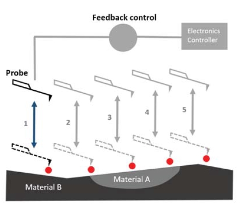
Fig. 2.A schematic representation of PinPoint mode operation. The probe approaches towards the sample surface until a pre-defined force threshold is reached, then the Z scanner height is recorded. The XY scanner stops and the piezoelectric response is measured. Then the probe retracts away from the surface and move to the next pixel. The process repeats to collect the topography map and the piezoelectric response map.
Experimental
A Park NX10 AFM was used to image the annealed phenanthrene surface, and the topography signal and PFM quad signal were acquired in both conventional PFM imaging and PinPoint™ PFM imaging. In conventional PFM imaging, a NSC36-C (nominal spring constant k = 0.6 N/m and resonance frequency f = 65 kHz) coated with Cr and Au on both the front and back side was used in conventional PFM imaging. The nominal radius of the tip curvature is ~25 nm. Scan size was 20 μm × 20 μm. Scan rate was 0.2 Hz. The AFM tip was biased with AC potential with an amplitude of 4.5 V and a frequency of 17 kHz. No external bias was applied to the sample during imaging. The force set point used in the experiment was 6.84 nN. In PinPoint™ PFM imaging, a conductive NANOSENSORS™ PointProbe® Plus-Electrostatic Force Microscopy (PPP-EFM) cantilever (nominal spring constant k = 2.8 N/m and resonance frequency f = 25 kHz) coated with Ptlr5 on both the front and back sides was used in PinPoint™ PFM imaging. The nominal radius of the tip curvature is ~25 nm. Scan size was 20 μm × 20 μm. Same as the conventional PFM experiment, a AC potential with an amplitude of 4.5 V and a frequency of 17 kHz was applied to the tip, and no DC potential was applied to the sample. The force set point used in the experiment was 196.8 nN. The retract height was 0.3 μm. The retract/approach speed was 20 μm/s. The contact time between the probe and the sample surface was controlled at 1 ms.
Results and Discussion
In Figure 3, the topography and the piezoelectric response maps of the annealed phenanthrene thin film on ITO surface imaged with both conventional PFM and PinPoint™ PFM are shown. The images obtained via conventional PFM are shown in Figure 3a (topography) and Figure 3b (piezoelectric response), and the images collected by PinPoint PFM are shown in Figure 3c (topography) and Figure 3d (piezoelectric response). From the topography images (Figure 3a and 3c), the annealed phenanthrene polymer was resolved under both imaging modes and observed to be rod-shaped features with pointy ends. The height of polymer rods was measured to be ranging from 50 to 400 nm, while the width of the polymer rods was measured to be between several hundred of nm to a couple of μm. It is noteworthy that the quality of the topography image obtained via PinPoint PFM is significantly improved compared to that taken with conventional PFM mode. In Figure 3c, under PinPoint PFM imaging conditions, the annealed phenanthrene polymer were well-distinguished from the ITO substrate. However, in Figure 3a, under conventional PFM imaging conditions, image artifacts can be seen throughout the entire scan area, indicating that the probe was scratching on the surface repeatedly. Of note, for conventional PFM measurement, our initial attempt was to use PPP-EFM (f = 2.8 N/m) as the probe, which is the same as the one used in the PinPoint PFM measurements. However, the probe was constantly scratching on the surface and the image quality was very poor. A cantilever with smaller force constant, NSC36-C (f = 0.6 N/m) was used instead, in hope to alleviate the scraping on the surface. Albeit the NSC36-C has a smaller force constant compared to that of PPP-EFM, the probe was still dragging on the surface and resulted in imaging artifacts as seen in Figure 3a. In PinPoint PFM, on the other hand, since the probe was retracted away from the surface to a safe height at every pixel prior to approach towards the surface, the scratching between the probe and the underlying substrate was effectively eliminated, leading to significantly improved imaging quality.
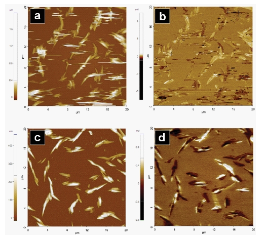
Figure. 3.a) Topography image taken with conventional PFM mode; b) PFM quad image taken with conventional PFM mode; c) Topography image taken with PinPoint PFM mode; d) PFM quad image taken with PinPoint PFM mode. Scan size: 20 μm × 20 μm.
Similar results were observed in the piezoelectric response images (Figure 3b and Figure 3d).By comparing the results of the two techniques, one can easily determine that PinPoint PFM has better performance compared to conventional PFM in the detection of piezoelectric response as the image obtained under PinPoint PFM was much better compared to that taken with conventional PFM mode.
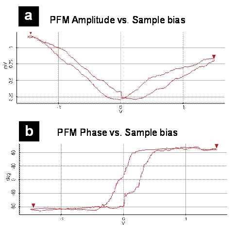
Figure. 4. Hysteresis curves for the amplitude (a) and phase (b) signal taken with the phenanthrene polymer film.
Figure 4a and 4b are hysteresis curves for the PFM amplitude and PFM phase signals of the phenanthrene film. These hysteresis curves were obtained by measuring the piezoelectric response at a specific location of the sample while applying the sample bias from -1.5 V to +1.5 V. The hysteresis curves provide localized information with respect to the switching properties of piezoelectric material. In Figure 4a, a characteristic “butterfly” shape that is similar to the ideal strain versus bias curve was observed in the amplitude signal. In addition, the coercive voltage, which is a measure of ability to withstand an external electric field without depolarization, is ~0.3 V. In Figure 4b, the phase hysteresis loop is shown, which is the typical response of a ferroelectric material.
Conclusions
Here in this application note, imaging performance of PinPoint PFM mode and conventional PFM mode was compared on phenanthrene film annealed on ITO surface. The PinPoint PFM mode introduced by Park Systems has proven to offer significantly-improved quality in both topography and piezoelectric response measurement. The advanced PinPoint mechanism eliminates the frictional force between the probe and the substrate, enabling concurrent high-resolution topography and piezoelectric response mapping of the surface. In addition, the response in strain (PFM amplitude) and polarization (phase) as a function of applied voltage was examined to obtain insights regarding material characteristics such as coercive voltage and hysteresis. Taken in total, PinPoint PFM mode is the ideal approach to characterize and quantify localized piezoelectric response at nanoscale, with maximized tip life and sample originality as a result of minimal frictional force between tip and sample.
References
[1] Ikeda T. Piezoelectricity. Oxford university press; 1990.
[2] Soergel E. Piezoresponse force microscopy (PFM). J Phys D Appl Phys. 2011;44(46):464003.
[3] Vijaya MS. Piezoelectric Materials and Devices: Applications in Engineering and Medical Sciences. CRC Press; 2012.
.