


Electrical Conductivity Measurement of Carbon Nanotubes Film using Conductive Probe Atomic Force Microscopy (C-AFM)
John Paul Pineda, Gerald Pascual, Byong Kim, and Keibock Lee Park Systems Inc., Santa Clara, CA USA
ABSTRACT
Electrical conductivity measurement is an effective approach to describe how a material behaves for certain applications, ranging from energy storage and energy conversion devices, to interconnections in molecular electronics and nanometer-sized semi-conductor devices. A technique known as Conductive Probe Atomic Force Microscopy (C-AFM) is a powerful technique that provides accurate nanoscale measurement and mapping of relative difference in electrical conductivity of advanced materials such as CNTs film. Several characterization techniques were introduced in the past decade to study these materials, however, majority of these can only measure a limited electrical properties range. In this study, Park NX20 equipped with C-AFM was used to investigate 3 different materials with wide range of electrical conductivity. The data acquired in this experiment clearly demonstrate the ability of this technique in measuring wide range of electrical conductivity and differentiating surfaces of materials covered with various types of conductive materials, with the use of a logarithmic current amplifier integrated in the system.
INTRODUCTION
Carbon Nanotubes (CNTs) have attracted a great deal of scientific attention and industrial interest world-wide due to its unique electrical behavior [1, 2]. A number of different applications ranging from energy storage and energy conversion devices, to interconnections in molecular electronics and nanometer-sized semi-conductor devices were demonstrated over the past decade [3, 4]. CNTs can behave as metallic or semi-conducting materials depending on the arrangement of their atoms, their chirality (degree of twist), as well as their sizes (diameter and length) [1, 2]. The electrical conductivity of CNTs plays a major role in describing its behavior and its implication to science and electronics. Therefore, it’s critically important to utilize a technique that can effectively measure the electrical conductive properties of these new materials. However, due to their fragile characteristics and nano-scale dimensions, measuring their local properties have become a great challenge to many researchers and device engineers [5, 6]. There are several methods that were introduced to characterize these materials, and the most common are scanning tunneling microscopy (STM), transmission electron microscopy (TEM) and focused ion beams (FIBs). [5, 7, 8] However, some of these techniques are destructive, some have a limited measurement and property characterization modes, others require high vacuum environment. One of the most powerful tools that was designed to overcome these problems is Conductive Probe Atomic Force Microscopy (C-AFM). This technique provides both electrical properties and topography at the same time, first by monitoring the current flowing between the conductive tip and sample, and the latter by monitoring the cantilever deflection as the tip scans over the sample surface.
In this study, Park NX20 equipped with C-AFM was used to investigate 3 different materials namely: 1) glass, 2) silver and 3) CNTs film. The results acquired in this experiment clearly demonstrate the ability of this technique to accurately measure wide range of electrical conductivity of advanced materials such as CNTs film. In addition, this technique can be used effectively to differentiate regions covered with various types of conductive materials.
EXPERIMENTAL
Sample and Probe
The sample that was investigated in this experiment is a CNTs film made of soot of carbon nanotubes that were deposited on a glass substrate to form a thin film layer. Subsequently, an Ag electrode is patterned into the surface to make an electrical contact. A conductive diamond coated probe (NANOSENSORS™ CDT-CONTR) with a nominal force constant of k = 0.5 N/m and resonance frequency of f = 20 kHz was utilized in the entire test.
C-AFM Experimental Conditions
The CNT film sample was investigated using Park NX20 AFM system under ambient air conditions to perform a 45 x 45 μm scan outputting to an image size of 256 x 256 pixels.Figure 1 shows the principles of C-AFM. The topography and electrical properties of the sample can be acquired simultaneously during operation. The topography data is acquired by monitoring the deflection signal of the cantilever as the conductive tip scans the sample surface in contact. On the other hand, electric conductivity is acquired by measuring the electrical current passing in between the conductive probe and the sample, produced by applying a bias voltage in between the two. The electrical conductivity is measured through an electric current amplifier. In this experiment, the bias voltage that was used is positive 0.3V, since the optimum current distribution was observed using this value. Generally, the current flow is acquired by a current amplifier and then processed into an image. The Park NX20 is equipped with internal current amplifier with variable gain of 106~1012 V/A, however, since the sample consists of different materials with wide range of electrical conductivity from nearly non conducting 0μAtorelatively well conducting 23.18μA, a logarithmic amplifier adaptable to this range was utilized in the experiment.
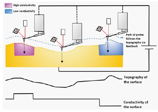
Fig. 1.Principles of Conductive Probe AFM. This diagram demonstrates that feedback control from the AFM controller allows this technique to acquire both surface topography and conductivity data simultaneously. The topography data is acquired by monitoring the deflection signal of the cantilever, while electric conductivity is acquired by measuring the tunneling current using current amplifier.
RESULT AND DISCUSSION
The acquired images were analyzed using XEI software developed by Park Systems which mapped the acquired signals to a color table. For topography image, the intensity of the shading correlates to the surface height variation with extremely bright and dark areas having the highest and lowest height regions. Figure 2shows the topography and current image of the CNTs film sample. The topography data clearly shows that the 45um by 45um scanned surface of the sample is composed of areas with variousheights which can be divided into 3 regions. It can be observed that the region with the lowest height has arelatively smooth surface, suggesting that this region is glass substrate. On the other, the two other regions have relatively rough surfaces, suggesting that these regions are the CNTs and Ag materials. The surface roughness of each regions were calculated using XEI software. The measured surface roughness of the glass substrate was approximately1.48 nm, while the other two regions have around 14.25 and 14.71 nm. Since the CNTs and Ag has almost the same features, differentiating these two materials will be difficult by simply looking at the topography data. The current image clearly differentiates the material composition of the sample and it also shows that the surfaces of the sample is divided into 3 regions. The areas with highest conductivity are represented by the red color map, while areas with lower conductivity are represented by the green color map, and for the areas that are non-conductive are represented by brown color map. Among the 3 materials, Ag has the highest conductivity, while CNT has 2nd to the highest, and the glass has the lowest conductivity [9].
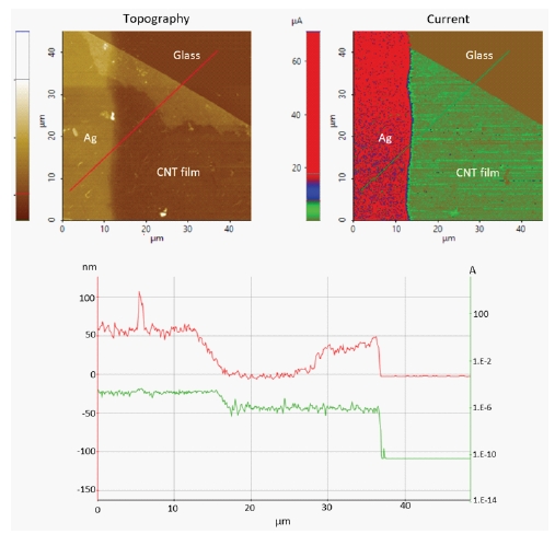
Fig. 2.Topography (top-left) and current image (top-right) acquired from CNTs film sample. Scan size: 45 x 45 μm, image size: 256 x 256 pixels.Topography line profile (red line, y-axis on left) and current line profile (green, y-axis on right).
If one were to analyze the corresponding line profile of topography and current image, the region with the highest height in topography image is the region with the highest conductivity in current image which is the Ag materials, while the region with 2nd to the highest height and conductivity is the CNTs film, and the lowest is the glass substrate. The quantitative results of conductivity in terms of measured current values are shown in the Table. The average measured conductivity of Ag is approximately 23.56 μA, while for CNT is 0.98 μA, and for glass is 0 μA. The results were plotted in Figure 3 to better analyze the data. The standard deviations of the electrical conductivity results were also calculated. The glass sample has the lowest standard deviation with Std = 0 A, while Ag sample has the highest standard deviation with Std = 8.
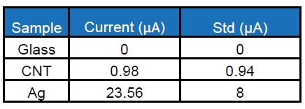
Table. 1.Measuredmean and standard deviation (Std) of current.
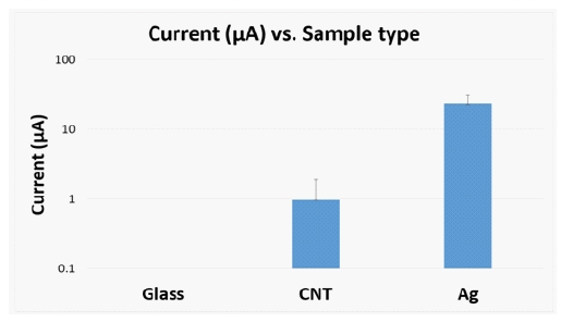
Figure. 3. Plotted value of measured mean standard deviation (Std) of current.
SUMMARY
The topography and electrical conductivity of a CNTs film have been characterized using C-AFM with a Park NX20 AFM system. The data collected in this experiment reveals that this technique can provide qualitative and quantitative information for electrical characterization of advanced materials. Moreover, the results demonstrate that this technique is an effective mean in measuring wide range of electrical conductivity and differentiating surfaces of materials covered with various types of conductive materials, with the use of a logarithmic current amplifier integrated in the system. Overall, the technique described in this study will successfully help researchers and device engineers with key electrical parameters information to better understand the behavior of certain material with unique properties such as CNTs
RESULT AND DISCUSSION
1.Y. Xue, Experimental Study of Electrical Conductivity of Carbon Nanotube, Nanofiber Buckypapers, and Their Composites.
2. P. Collins, et al., The Electronic Properties of Carbon Nanotubes.
3. J. Brito, et al., Nanostructured films from phthalocyanine and carbon nanotubes: Surface morphology and electrical characterization. Journal of Colloid and Interface Science, Volume 367, Issue 1, 1 February 2012, Pages 467-471.
4. J. Maklin, ELECTRICAL AND THERMAL APPLICATIONS OF CARBON NANOTUBE FILMS
5. Z. Wang, et al., Measuring physical and mechanical properties of individual carbon nanotubes by in situ TEM. Journal of Physics and Chemistry of Solids 61 (2000) 1025–1030.
6. M. Li, et al., Analysis of variance on thickness and electrical conductivity measurements of carbon nanotube thin films. Published 19 July 2016 • © 2016 IOP Publishing Ltd, Measurement Science and Technology, Volume 27, Number 9.
7. K. Lee, Failure analysis and the innovative PinPoint™ conductive AFM
8. G. Homyak, et.al, TEM, STM and AFM as tools to study clusters and colloids. Micron, Volume 29, Issues 2–3, April–June 1998, Pages 183-190. https://doi.org/10.1016/S0968-4328(97)00058-9
9. A. Helmenstine, Table of Electrical Resistivity and Conductivity.