


John Paul Pineda, Gerald Pascual, Byong Kim, and Keibock Lee
Park Systems Inc., Santa Clara, CA, USA
Introduction
The need to measure sample surface features have become increasingly important in many applications such as manufacturing semiconductor devices and monitoring the structural characteristics of biological samples. There are some AFM techniques used in measurement of sample topography. Examples include tapping mode and contact mode. However, these modes require a tip-sample interaction that can lead to sample damage and tip quality degradation. The need for a technique that can measure surface topography without touching the sample surface is very real, especially for samples sensitive to surface deformation.
The True Non-Contact imaging mode of AFM systems from Park Systems addresses this problem by allowing the acquisition of surface topography without the AFM tip touching the sample. The advanced Z scanner design of Park AFM is the key feature in achieving the non-contact imaging performance that defines Park's True Non-Contact mode: the highest imaging resolution and most accurate topographical data whilst maintaining tip sharpness and minimizing the chance of damaging the sample surface. In this paper, different samples were measured to evaluate the performance of Park AFM and its unique approach to non-contact imaging.
Experiments
Different types of samples were investigated using the Park XE7 AFM system to evaluate the tool's True Non-Contact mode performance. These samples were characterized under ambient air condition in the following sequence: 1) a sapphire wafer, 2) a tungsten film, and 3) collagen fibrils. The sapphire wafer was the first sample to be measured in order to check the performance of the Park XE7's low noise detectors in measuring samples with nanoscale features. With that check completed, the tungsten film and collagen fibrils were then measured to prove that there is no physical contact between the tip and the sample during scanning. The same cantilever with a relatively high resonance frequency ~300 kHz and spring constant ~ 40 N/m was utilized in measuring the samples in the entire process.
The non-contact AFM image is acquired by measuring the changes in the vibrational amplitude of the cantilever induced by the attractive van der Waals Force as the cantilever is mechanically oscillated near its resonant frequency during the scan. The measured changes are compensated by the AFM's feedback loop which maintains the cantilever's constant amplitude and distance. Non-contact mode measures the topography of the sample surface by using this feedback mechanism to control the Z scanner movement [1]. In this study, the constantly maintained amplitude (or set-point) was selected based on the characteristics of each samples. Theoretically, the closer the value of the set-point to the driving amplitude, the larger the distance between the tip and the sample. The set-point selected for tungsten film is around 80% of the driving amplitude. A higher set-point was chosen for this sample to ensure the tip did not touch the surface. Since a tungsten film surface is harder than the silicon tip, the tip-sample interaction would lead to severe tip damage. For the sapphire wafer and collagen fibril, the set point was chosen to be lower, around 40 – 50% of the driving amplitude, since better resolution can be acquired within this range.
RESULTS & DISCUSSIONS
Sapphire wafers are widely used as substrates for various nanostructured devices [2] [3]. The performances of the materials that are grown on them are influenced by its surface; the step formation in the surface can greatly affect the growing quality. Thus, it is important to monitor the step formation in the manufacturing process to attain a defect-free, smooth surface. Figure 3 illustrates the atomic steps of a sapphire wafer and its corresponding line profile generated after scanning. The line profile clearly shows that a 2 nm step height is present in the sample surface. Such small measurements can only be acquired by AFMs that are equipped with low noise Z height measurement capability. The Park XE7 that was used in this experiment has Z height detection capable of functioning correctly with a noise level of up to 0.02 nm. This noise level is low enough to acquire an accurate topographical measurement at nanoscale.
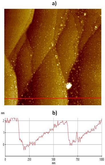 Figure 1. (a) Non-contact AFM topography image of a sapphire wafer sample using True Non-Contact mode from Park Systems. Scan size: 1 x 1 μm, image size: 256 x 256 px. (b) Non-contact AFM topography line profile using True Non-Contact mode from Park Systems.
Figure 2a and 2b show the tungsten film images measured in two different scans. The image in Figure 2a was acquired during the 1st scan while Figure 2b was acquired in the 10th scan. Although the same tip was used for all scans, the results show a high resolution image can still be acquired even after several measurements have been performed in Park's True Non-Contact mode. This proves that Park's solution preserves the tip sharpness by acquiring image without tip-sample interaction. AFM tips are known to be brittle and it is reasonable to expect them to be blunted upon contact with hard samples such as tungsten film. Blunt AFM tips can no longer sense the sample surface with the same resolution as fresh tips; if this were the case with Park's True Non-Contact mode, the 10th scan should have been of significantly lower quality.
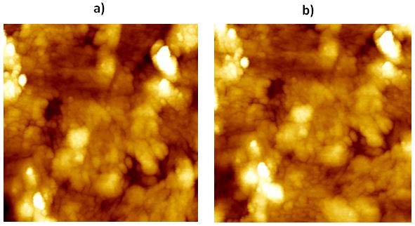 Figure 2. (a) Non-contact topography AFM image (1st scan) of a tungsten film sample using True Non-Contact mode from Park Systems. Scan Size: 1 x 1 μm, Image size: 256 x 256 px. (b) Non-contact topography AFM image (10th scan) of a tungsten film sample using True Non-Contact mode from Park Systems. Scan size: 1 x 1 μm, image size: 256 x 256 px.
Imaging biological samples such as collagen fibrils have drawn much attention to researchers due to a combination of their nature of being easily damaged and that most of the characterization techniques available are destructive. The True-Non Contact imaging of Park AFM addresses this problem by allowing users to acquire accurate and high resolution images without touching the sample.
Figure 3a and 3b shows the topography and phase images of collagen fibrils. The images revealed that the structure of a single fibril consists of segments which align parallel to one another. The D-gap which appears to be darker in between the segments is also clearly visible in the image. The accurate characterization of collagen fibril structure is relevant in many scientific applications especially in biomedicine [4] [5] [6].
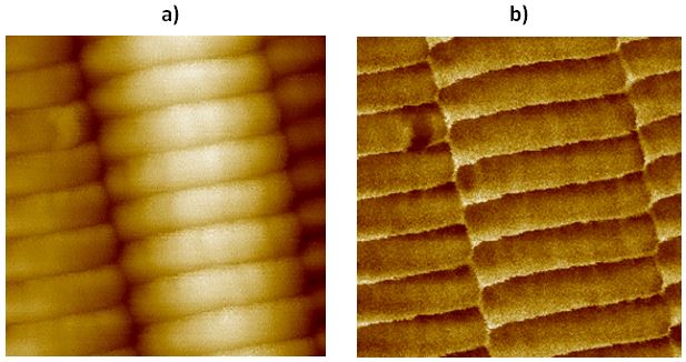
Figure 3. (a) Non-contact AFM topography image of collagen fibrils using True Non-Contact mode from Park Systems. Scan size: 500 x 500 nm, image size: 256 x 256 px. (b) Phase image of collagen fibrils using True Non-Contact mode from Park Systems. Scan size: 500 x 500 nm, image size: 256 x 256 px.
SUMMARY
The topography of a sapphire wafer, tungsten film, and collagen fibrils have been efficiently and accurately imaged using non-contact AFM on the Park XE7 AFM system. The results show the True Non-Contact mode of Park AFM is an effective means of measuring surface properties and topography without touching the sample surface with an AFM cantilever tip. The key in True Non-Contact imaging is the Z-scanner design with high Z-feedback system. True Non-Contact mode from Park Systems successfully provides researchers with the means to characterize their samples' surfaces at nanoscale level with the highest resolution and accuracy possible, free from any worry about tip blunting or tip-induced sample damage.
REFERENCES
[1] Park AFM Modes and Techniques. (n.d.). Retrieved October 18, 2016, from http://www.parkafm.com/index.php/park-afm-modes
[2] Y. Li, et al., Defect-reduced green GaInN/GaN light-emitting diode on nanopatterned sapphire. Appl. Phys. Lett. 98, 151102 (2011)
[3] G. Wang, et al., Highly aligned, template-free growth and characterization of vertical GaN nanowires on sapphire by metal–organic chemical vapour deposition. Nanotechnology, Volume 17, Number 23
[4] S. Yamamoto, et al., Observation of Human Corneal and Scleral Collagen Fibrils by Atomic Force Microscopy. Japanese Journal of Ophthalmology, Pages 496–501