


Hosung Seo, Dan Goo, and Gordon Jung
Performance Testing Team, R&D Center, Park Systems Corporation
INTRODUCTION
Kelvin Probe Force Microscopy, or KPFM, was introduced as a tool to measure the local contact potential difference between a conducting atomic force microscopy (AFM) tip and the sample, thereby mapping the work function or surface potential of the sample with high spatial resolution. Since its first introduction by Nonnenmacher [1], KPFM has been used extensively as a unique method to characterize the nano-scale electrical properties of metal or semiconductor surfaces and semiconductor devices. Recently, KPFM has also been used to study the electrical properties of organic materials, devices [2–4] and biological materials. To eliminate any confusion, let us look into KPFM’s synonyms for this technique:
- KPFM: Kelvin Probe Force Microscopy
- SKPM: Scanning Kelvin Probe Microscopy
- SSPM: Scanning surface potential Microscopy
- SKFM: Scanning Kelvin Force Microscopy
- SPM: Surface Potential Microscopy
- SP-AFM: Surface Potential Atomic Force Microscopy
KPFM will be used in this document, as it is the most widely used descriptor for this technique. The term ’Kelvin force’ refers to similarities between this microscopic technique and the macroscopic technique, which is the Kelvin probe method. However, the methodology is somewhat different, but the measured value is equivalent for both techniques. For clarity, this note will refer only to the microscopic technique KPFM.
Fundamentals of KPFM
The KPFM measures Contact Potential Difference (CPD) between a conducting AFM tip and a sample. The CPD (VCPD) between the tip and sample is defined as:
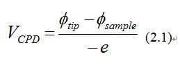
where ϕsample and ϕtip are the work functions of the sample and tip, and e is the electronic charge. The different Fermi energy levels between the AFM tip and sample surface causes an electrical force as the AFM tip is brought close to the sample surface. Fig. 1 shows the energy level diagram of the tip and sample surface when ϕsample and ϕtip are different. Fig. 1(a) depicts the energy levels of the tip and sample surface when the tip and sample surface are separated, yet close enough for electron tunneling; equilibrium of the states require Fermi levels to line-up at steady state. Upon electrical contact, the Fermi levels will align through electron current flow, and the system will reach to an equilibrium state as shown in Fig. 1(b). The tip and sample surface will be charged, and an apparent VCPD will be formed (note that the Fermi energy levels are aligned but the vacuum energy levels are no longer the same, and a VCPD between the tip and sample has been formed). An electrical force acts on the contact area, due to the VCPD. As shown in Fig. 1(c), this force can be nullified. This technique is the Kevin Probe method that relies on the detection of an electric field between a sample material and a probe material. The electric field can be varied by the voltage VCPD, that is applied to the sample relative to the probe. If an applied external bias (VDC) has the same magnitude as the VCPD with opposite direction, the applied voltage eliminates the surface charge of the contact area.
The applied VCPD nullifies the electrical force and has the same value as the work function difference between the tip and the sample. This allows the work function of the sample to be calculated when the work function of the tip is known.
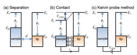
Figure 1. Electronic energy levels of the sample and AFM tip for three cases: (a) tip and sample are separated by distance d with no electrical contact, (b) tip and sample are in electrical contact, and (c) external bias (VDC) is applied between tip and sample to nullify the CPD and, therefore, the tip-sample electrical force. Ev is the vacuum energy level. Efs and Eft are Fermi energy levels of the sample and tip, respectively.
By applying an AC voltage (VAC) plus a DC voltage (VDC) to the AFM tip, KPFM measures the work function of the sample. VAC generates the oscillating electrical forces between the AFM tip and sample surface, and VDC nullifies the oscillating electrical forces that originated from CPD between the tip and the sample surface. The electrostatic force (Fes) between the AFM tip and sample is given by:
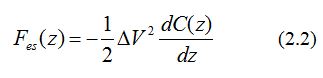
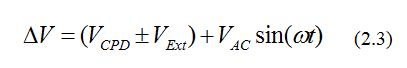
where z is the direction normal to the sample surface, ΔV is the potential difference between VCPD and the voltage applied to the AFM tip, and dC/dz is the gradient of the capacitance between tip and sample surface. The external potential, VExt, is an additional voltage that is applied either to the tip or to the sample; the sign in front of VExt is explained below. The voltage difference ΔV will be [5]:
The amplitude of the tip vibration, VAC, is proportional to the force F. Substituting the expression of the voltage given in Eq. (2.2) in Eq. (2.3) and collecting the terms according to their frequencies, the following form for the amplitude of the tip vibration is obtained:
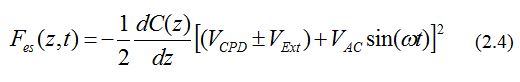
This equation can be divided into three parts:
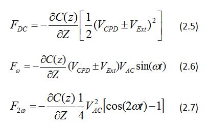
FDC (Eq. (2.5)) results in a static deflection of the AFM tip. Fω with frequency ω (Eq. (2.6)) is used to measure the VCPD, and F2ω is used for capacitance microscopy [6]. Fω is the electrical force component modified with frequency ω. It is also the function of VCPD and VAC. When electrostatic forces are applied to the tip by VAC with VExt, additional oscillating components (due to the electrical force) will be superimposed to the mechanical oscillation of the AFM tip. A lock-in amplifier is employed to measure the VCPD and enable the extraction of Fω. The output signal of the lock-in amplifier is directly proportional to the difference between VCPD and VExt. The VCPD value can be measured by applying VExt to the AFM tip, such that the output signal of the lock-in amplifier is nullified and Fω reaches to the zero. Subsequently, the value of VExt is obtained for each point on the sample surface and maps the work function or surface potential of the whole sample surface area. The contact potential difference, VCPD, is obtained by the following procedure: the direct current VDC voltage, VExt, is varied until the alternating current VAC vibration of the tip at the frequency ω is nullified; at this voltage VExt=±VCPD.
When the external voltage is applied to the tip or to the sample it changes their work functions. Hence, based on Eq. (2.1) the sign of VCPD will be different in the two cases. The posteriori DC voltage difference (direction)VCPD is thus given for the two cases as:
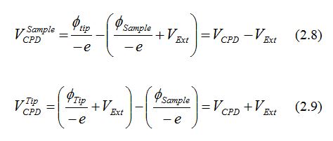
where Eq. (2.8) and (2.9) are for the cases of voltage applied to the sample and the tip, respectively and VCPD is nullified with an external bias, i.e., when VExt=±VCPD, where the ‘+’ and ‘-’ refer to the external bias applied to the sample and the tip, respectively.
KPFM mode for Park Systems
There are various methods of measuring the KPFM mode in AFM. Park Systems uses two frequencies as showed in Fig 2. In the controller, wwo lock-in amplifiers are implemented for frequency modulation: one frequency is used to oscillate the cantilever and obtain a surface image using Bimorph, which is the term for oscillating the cantilever using piezo electric material, and the second frequency directly amplifies the cantilever signal at 17.0 kHz, which is the frequency generally used for KPFM.
The topography signal and potential signal are acquired from each frequency simultaneously and two images are created independently, allowing the user to obtain a surface image and a potential image simultaneously. The topography signal is obtained by keeping the distance constant between the tip and sample, whereas the potential image is obtained by applying a default external voltage and potential measurement voltage on the cantilever as described in Figure 2.
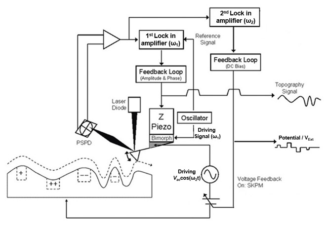
Figure 2. KPFM schematic used by Park Systems. Fig. 3 (e) is the line profile data of the mean values for 16 adjacent points along the y-axis. It can be seen in the metal regions in the potential difference (Vext) image that they are mutually inverted. This proves that the inverted signs, positive and negative expressions, in Eq. (2.8) and (2.9) are correct.
To perform a KPFM measurement of a sample patterned with Si-Al-Au, the NANOSENSORS NCHAu cantilever was chosen. This cantilever has a metallic layer coated on both sides of the cantilever and has a typical tip radius of curvature smaller than 50 nm. The resonant frequency and force constant are 330 kHz and 42 N/m, respectively. Since the tip and surface are dissimilar materials, the voltage offset between the tip and the surface sample may occur as shown in Fig. 3(e). To perform KPFM, this offset, which originates from the VAC amplitude, must be quantified. Therefore, it is necessary to measure a calibration sample, such as highly oriented pyrolytic graphite (HOPG), which has a known work function. It should be noted that the difference between the Au and Al areas must be constant according to the applied direction because there is an absolute difference in work function.
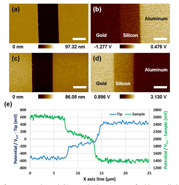
Figure 3. (a) Surface topography and (b) VExt in the presence of a bias applied normal to the sample surface in the upward direction. Similarly, (c) surface topography and (d) VExt in the presence of a downward bias. (e) Line profiles of VExt (potential differences) with a bias in the upward (blue) and downward (green) directions. All images are 25.0 µm x 12.5 µm. Scale bar: 5 µm.
Fig. 3 (e) shows the line profile data of the mean values for 16 adjacent points along the y-axis. The metal regions exhibit a switch in the potential difference (Vext) and invert, corroborating the positive and negative expressions found in Eq. (2.8) and (2.9).
Analysis & Repeatability of KPFM
The purpose of KPFM is to obtain the work function of the specimen, not the VCPD between the tip and the sample. Calibration of the system must be performed by using a sample with a known work function for reference. Using this reference, the work function must be measured to eliminate the potential for electrical offset that can occur during a KPFM measurement. After measuring the KPFM of the sample, the work function of the tip is obtained by using Eq. (2.10). Finally, repeating this process several times and averaging the results using several cantilevers will produce accurate results.
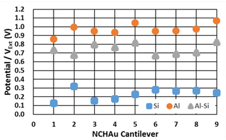
Figure 4. KPFM data obtained using nine different NCHAu (NANOSENSORS) probes on the Au-Si-Al patterned sample. The values on Al (orange circles), Si (blue square) and their differences (gray triangles) are plotted.
The sample consisted of three different materials; Au, Si, and Al. For the calibration, Au was selected as a reference since the cantilever was Au coated and made of the same material. The work function of Si and Al were determined as explained above. The theoretical work function values and the experimentally determined work function values of Si and Al are shown in Table 1.
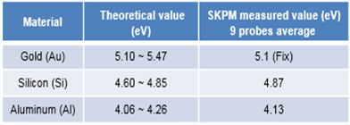
Table1. Theoretical work function values and the average work function values (n = 9 cantilevers).
Park Systems offers a suite of KPFM measurement analysis, Ultimately, KPFM has brought us a quantitative sample’s work function measurement.
REFERENCES
[1] M. Nonnenmacher, M.P. Oboyle, H.K. Wickramasinghe, Appl. Phys. Lett. 58(1991) 2921.
[2] H. Hoppe, T. Glatzel, M. Niggemann, A. Hinsch, M.C. Lux-Steiner, N.S. Sariciftci, Nano Lett. 5 (2005) 269.
[3] T. Hallam, C.M. Duffy, T. Minakata, M. Ando, H. Sirringhaus, Nanotechnology 20 (2009) 025203.
[4] L.M. Liu, G.Y. Li, Appl. Phys. Lett. 96 (2010) 083302.
[5] R. Shikler, T. Meoded, N. Fried, B. Mishori, Y. Rosenwaks, J. Appl. Phys. 86 (1999) 107.
[6] S.V. Kalinin, A. Gruverman (Eds.), Scanning Probe Microscopy, Springer, New York, 2007.