


 "Park Systems is excited to offer this luncheon seminar that demonstrates how our engineering and product development team is focused on failure analysis solutions for the manufacturing environment towards the advancement of nanoscale production."
Santa Clara, CA June 22, 2015
Park Systems, a leader in Atomic Force Microscopy (AFM) since 1997 is hosting a SEMICON West Luncheon titled SSRM Imaging of Semiconductor Devices with High Spatial Resolution and Electrical Sensitivity Using an AFM Operating in a Vacuum, by Phani Kondapani, Park Systems Technical Engineer. The luncheon, open to all SEMICON West attendees and Park customers will be held from 12:00p to 2:00p on Wednesday, July 15th on the 2nd floor of the ThirstyBear Brewing Company located on 661 Howard Street, San Francisco, less than a 5-minute walk from South Hall of the Moscone Center. Park Systems will be exhibiting this year in booth 2041at SEMICON West where you can learn more about Park NX-Hivac, along with all of Park Systems AFM innovations for the Semiconductor industry, including the next generation automated 3D-AFM, under joint development with imec, and Park SmartScan, a revolutionary automated AFM software system for professional AFM images with a single Click. To register for the free luncheon, go to: http://www.parkafm.com/semiconwest
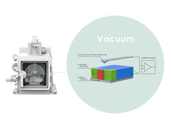
"SSRM (Scanning Spreading Resistance Microscopy) has become the choice technique for two-dimensional carrier profiling in ultra-small semiconductor devices," explains Phani Konpdapani. "However, because the device surface readily forms an unwanted layer of oxide and hydrocarbon in air, it has been difficult to achieve high spatial resolution and electrical sensitivity in images while maintaining measurement repeatability."
To overcome this challenge, Park Systems has developed Park NX-Hivac, a new AFM tool that is capable of acquiring SSRM data in a vacuum. Park NX-Hivac is already being well accepted in stringent semiconductor test environments. Those experimental results prove that NX-Hivac's SSRM data can achieve repeatability not only with nanoscale spatial resolution but also with electrical sensitivity that can differentiate a wide range of dopant concentration across 7 decades.
Park NX-Hivac is ideal for academic and industrial customers who are interested in failure analysis solutions in highly doped semiconductor processes where more highly sophisticated tools are now required. Park's commitment to superior products that enhance the customer's performance led to the development of Park NX-Hivac, which was designed in collaboration with a major semiconductor IC producer. The high vacuum scanning spreading resistance microscopy of Park NX-Hivac enables 2D carrier profiling of next generation devices and produces high resolution SSRM images under high vacuum conditions to minimize sample-tip damage and improve production yield. Park NX-Hivac is very sensitive and responsive to the current signal for accurate measurement and repeatability.
Mr. Phani Kondapani, who has a BS in Electrical Engineering and MS in Nanoscience, is one of many Technical Support Engineers at Park Systems who provide technical and applications support for innovative cutting-edge Park Atomic Force Microscope products to academia and industry nanotechnology research customers. The luncheon is one of an ongoing series of shared knowledge seminars that Park Systems hosts to deliver cutting edge, technology support across the industry groups they serve.
"Park Systems is excited to offer this luncheon seminar that demonstrates how our engineering and product development team is focused on failure analysis solutions for the manufacturing environment towards the advancement of nanoscale production," comments Keibock Lee, President of Park Systems. "Over the years, we have consistently outpaced our competition with innovations that provide value and accuracy for Semiconductor Manufacturing and this year is no exception as we add NX-Hivac to our arsenal of AFM tools for cutting edge wafer production."
With an expected attendance of over 25,000 visitors, SEMICON West is the premier annual event for the global microelectronics industry, highlighting the latest innovations, products, processes, and services for the design and manufacture of today's most sophisticated electronics. You will find Park Systems exhibit at the SEMICON West 2015 Show at booth 2041in Moscone Center South Hall.
About the Luncheon:
Park Systems is hosting a Free Luncheon on July 15 at the Thirsty Bear from 12-2pm featuring a seminar titled SSRM Imaging of Semiconductor Devices with High Spatial Resolution and Electrical Sensitivity Using an AFM Operating in a Vacuum given by Phani Kondapani, AFM Engineer. Anyone interested in Failure Analysis methods in Semiconductor Manufacturing is invited to attend.
Please register at: http://www.parkafm.com/semiconwest
About Park Systems
Park Systems serves its customers by providing a complete range of AFM solutions including AFM systems, options and software, along with global service and support. Park Systems is the leading nanotechnology solutions partner for nanoscale measurements and systems for both research and industry. The product line of Park Systems reflects its focused strength to help customers achieve the metrology performance that meets the needs and requirements of present and future applications. Since improvements in nanometrology are key to enabling tomorrow's research, analysis, processing and product manufacturing, the innovative technology and market leadership of Park Systems in the field of nanometrology will remain as the core competence and market driving force of its future business. Park's manufacturing and engineering facilities are located in Suwon, South Korea. Global sales and service offices are located throughout the U.S., Japan, and Singapore. For more information, visit http://www.parkAFM.com.