


 "We are grateful for the opportunity to partner with IMEC in a Joint Development Project.This partnership between Park Systems and imec provides a crucial link of scientific collaboration." Dr. Sang-il Park, CEO of Park Systems
Santa Clara, CA February 24, 2015
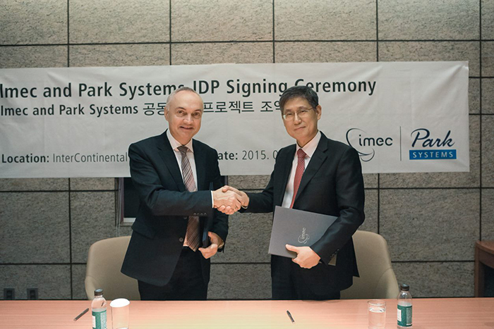
Park Systems, world-leader in Atomic Force Microscopes (AFM) announced today they have signed a Joint Development Project (JDP) with nanoelectronics research center imec, to develop in-line AFM metrology solutions of future technology nodes including but not limited to surface roughness, thickness, critical dimension (CD), and sidewall roughness. The JDP will develop new protocol designed to increase production yield and device performance for the semiconductor industry. Park Systems has officially joined imec's Industrial Affiliation Program (IIAP) and become a new member of IIAP at a signing ceremony in Seoul Korea on Feb 3, 2015.
"We are grateful for the opportunity to partner with IMEC in a Joint Development Project," comments Dr. Sang-il Park, CEO of Park Systems. "This partnership between Park Systems and imec provides a crucial link of scientific collaboration throughout the chain of suppliers and vendors in semiconductor wafer production. Significant future technological advances will be made from this JDP for AFM-based inline nanoscale metrology."
The partnership will develop a broad range of AFM metrology solutions for process development, production, and failure analysis. For surface roughness, the most accurate surface roughness measurement with wafer mapping and incoming material monitoring could be delivered. For thickness, accurate thickness value in pre- and post-processing will be delivered in order to complement the existing ellipsometry solution.
More importantly, the partnership will explore a new frontier of high resolution 3D AFM metrology to address accurate CD, line width roughness (LWR), line edge roughness (LER) measurements, and sidewall roughness during etch, EPI, film deposition, and lithography processes.
The JDP between Park Systems and imec will develop new in-line monitoring and analysis methods for semiconductor manufacturers as well as new production protocol for better process development and control, which will result in improved device performance and production yield. For example, the high resolution sidewall information on vertical planar and cylindrical structure by Park's new 3D AFM will bring huge impact on the performance of vertical devices such as FinFET, TFET, STT-MRAM and others.
As the design rule of semiconductor device shrinks, the CD measurement and sidewall variation in LER/LWR measurements became important and directly correlated with the leakage, hence device performance. CD-SEM, TEM, and OCD have been used for the CD metrology, but each technique has its shortcomings such as resolution and e-beam damage for CD-SEM, sample preparation and sample damage for TEM, and time-consuming process development for OCD. Now, the AFM enabled hybrid metrology is on the rise as the next generation in-line monitoring and analysis method of non-destructive CD control. In the most recent decade, the predictive power and correlation of the new hybrid metrology saw a vast improvement, and Park's new 3D AFM metrology will contribute the detailed sidewall and nanoscale surface information for the critical components in the yield control matrix. The collaboration between Park Systems and imec will create an information gathering platform from a multi disciplinary team of leading experts of scientists, engineers, and researchers to work together to create the next generation solutions in semiconductor metrology .
About Park Systems
Park Systems is a world-leading manufacturer of atomic force microscopy (AFM) systems with a complete range of products for researchers and industry engineers in chemistry, materials, physics, life sciences, semiconductor and data storage industries. Park's products are used by over a thousand of institutions and corporations worldwide. Park's AFM provides highest data accuracy at nanoscale resolution, superior productivity, and lowest operating cost thanks to its unique technology and innovative engineering. Park Systems, Inc. is headquartered in Santa Clara, California with its global manufacturing, and R&D headquarters in Korea. Park's products are sold and supported worldwide with regional headquarters in the US, Korea, Japan, and Singapore, and distribution partners throughout Europe, Asia, and America. Please visit http://www.parkafm.com or call 408-986-1110 for more information.