


An Interview with Park Systems AFM Customer, Dr. Ahmed Busnaina
Director, NSF Nanoscale Science and Engineering Center for High-rate Nanomanufacturing at Northeastern University
Northeastern University’s Center for High-rate Nanomanufacturing has developed a fully-automated system that uses offset-type printing technologies at the nanoscale to make products that fully take advantage of the superior properties of nanomaterials. In minutes, the system can print metals, organic and inorganic materials, polymers, and nanoscale structures and circuits (down to 25 nanometers) onto flexible or inflexible substrates. The Nanoscale Offset Printing System (NanoOPS) is a new system that has the potential to transform nanomanufacturing and spur innovation. Because of its relative simplicity, NanoOPS is expected to eliminate some of the high cost entry barriers to the fabrication of nanoscale devices for electronics, energy, medical, and functional materials applications. Current nanofabrication facilities cost billions of dollars to build, and their operation requires massive quantities of water and power. NanoOPS could operate at a fraction of the cost, making nanomanufacturing accessible to innovators and entrepreneurs and creating the potential for a wave of creativity, perhaps similar to what the PC did for computing and what the 3D printer is doing for design. In addition to reducing manufacturing costs, NanoOPS will go beyond current fabrication capabilities by enabling the commercialization of nanoscale properties, such as nanotubes, that have been identified in laboratory settings. This will enable critical manufacturing in areas such as new and more affordable medicines; stronger, lighter building materials; or faster, cheaper electronics.
What key benefits are offered by nanoOPS to the nanoscale manufacturing process?
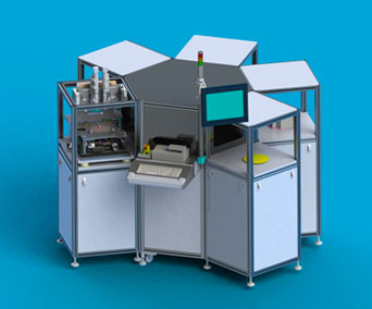 Nanoscale Offset printing System NanoOPS
Commercial nanoscale electronic device manufacturing is still largely top-down, silicon-based, and expensive. In addition, few nanoscale devices manufactured today exploit the unique properties and behaviors of nanomaterials such as nanotubes, quantum dots, and nano particles. Printing offers a novel approach to fabricating devices and products incorporating nanomaterials. Electronic printing today is used for making low-end electronics, however, these products are made using inkjet technology, which is very slow and limited to only micro scale resolution. Even with today's slow electronic printing and lower resolution, they still offer significant savings compared to silicon electronics. For example, the cost of a printed integrated sensor-plus-digital-readout device is 1/10th to 1/100th the cost of current silicon-based systems. The printed electronic market is close to $50 billion this year and is projected to reach $250 billion in 10 years. This is based on current electronic printing capability, however, if printing can be used to print high-end electronic devices at the same price but orders of magnitude faster, we think that the market will many times larger in the near future. Our new Nanoscale Offset printing System (NanoOPS); has been shown to be capable of being orders of magnitude faster and higher resolution than current inkjet based electronic printing and 3D printing. Our unique fully-automated NanoOPS that can be flexibly adapted to print a variety of micro- to nano-scale devices for many applications including electronics, energy, medical and functional materials.
What is an example of a nanoscale device that makes a difference in our daily lives?
There are applications that utilize nanomaterials such as nanoparticles, carbon nanotubes (CNTs) and Quantum Dots (QDs) but not at the nanoscale. For example, many printed electronics as well as organic photovoltaics utilizes nanomaterials using printing or roll-to-roll process. In addition, some large LCDs have already utilized QDs to display bright colors. However, all of these are low end application of nanomaterials. Once scalable high-rate nanoscale printing becomes available, then we will see a paradigm shift in the use of nanoscale devices produced with nanomaterials.
How does NanoOPS provide a solution for nanomanufacturing?
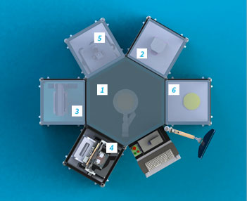 NanoOPS includes six modules:
1. Hexagon Frame Module
2. Template Load Port Module
3. Directed Assembly Module
4. Mask Aligner Module
5. Transfer Module
6. Template Load Port Module
This spring, we are taking some of our key discoveries to date out of the lab and into the marketplace. In collaboration with a Massachusetts-based company, the CHN has developed a unique fully-automated system: Nanoscale Offset Printing System (NanoOPS) that can be flexibly adapted to print a variety of micro- to nano-scale devices for many applications including electronics, energy, medical and functional materials. This one of a kind fully automated cluster tool printing system will be unveiled in September this year. The hexagonal machine is about seven feet across and has a central robotic arm that transfers the printing templates and the final products that will result from the precision multi scale manufacturing process.
If there's a key differentiator between past approaches and your own to high-throughput manufacturing at the nanoscale, what would it be?
The NanoOPS system will be fast, scalable, and capable of printing multiscale structures using a wide variety of functional nanomaterials at very low facilities and operational cost. This new system will transform nanomanufacturing and nano-enabled technologies and spur innovation by overcoming the high cost entry barrier to the fabrication of high-end printed devices at a fraction of today's cost. Although the flexible Damascene templates can be used in Roll-to-Roll printing system, NanoOPS utilizes a batch process to be able to apply nanoscale registration and alignment. The vision is to "democratize" nanomanufacturing, making it more broadly accessible to industry and entrepreneurs and unleashing a wave of creativity for nano-enabled product innovation - analogous to what the advent of the personal computer did for computing.
How is AFM (Atomic Force Microscopy) used ?
One of the many examples where the AFM could provide a unique and useful information(without sample damage) is regarding the alignment of single walled or multi walled carbon nanotube (SWNTs or MWNTs) structures which affects conductivity of the assembly (very significant for electronic or sensor applications) as well as for structural or composite materials applications. Below is an example of how the alignment of SWNTs can be controlled during directed assembly (using a dip coater). The AFM measurements clearly showed that the angle of assembled SWNTs is a function of pulling speed (as shown in the AFM image of assembled SWNTs at different pulling conditions).
What sets AFM apart from other forms of microscopy for your approach’s needs?
The AFM is capable of characterizing nanomaterials assembled in a 2D or 3D structure or just on a surface. SEM and other vacuum approaches can provide measurements with affecting the sample either because of the e-beam that will damage nanomaterials such as CNTs if exposed (more than few seconds at high magnification. Also, in the SEM, typically organics that accumulates in the chamber end up depositing on the substrate affecting and damaging the sample. Charging of samples also occurs and could cause sample damage. The AFM does not have any of these drawbacks. In addition, the quantitative measurements capabilities such as the 3D mapping of nanostructures cannot be matched by other techniques.
Can you explain what is meant by the Missing Middle in the Manufacturing process?
This is an excellent question and one that the US government has to pay attention to. Most of university research and breakthrough technologies get published and patented and then if no company licensed the technology or no spin off company is launched, the technology will not be commercialized. There is no mechanism for funding such the missing middle. Large companies like to buy a complete solution such as a start up that already built prototype and has developed the necessary echnology and filed the necessary patents needed for commercialization. However, a company has to be lunched and funded for a few years before that point is reached. Venture capitals and angel investor have been very conservation during the last decade. The new Advanced anufacturing institutes were supposed to provide a solution top this problem, but so far the institutes have focusing on improving or refining existing technology and less on developing emerging technology.
Note: The US Government Accountability Office (GAO) released a 100+ page report early this year on the state of nanomanufacturing in America that addressed the concern regarding the lack of funding or middle-stage support from initial proofs-ofconcept in laboratory settings to full-scale manufacturing which leads to many promising nanotechnology ideas dying on the vine before they can reach their full potential.
What advances in highrate nanomanufacturing do you envision in the near future?
New nanomaterials based manufacturing techniques are finding more acceptance and more companies are using or considering them. Among those are electronic printing with a market close to $50 billion. Even with today’s slow electronic printing and lower resolution, they still offer significant savings compared to silicon electronics. Printing, however, can be used to print or nanomanufacturehigh-end electronic devices at the same price but orders of magnitude faster. Our new Nanoscale Offset printing System (NanoOPS) has been shown to be capable of being orders of magnitude faster and higher resolution than current inkjet based electronic printing and 3D printing. This unique fullyautomated NanoOPS that can be flexibly adapted to print a variety of micro- to nano-scale devices for many applications including electronics, energy, medical and functional materials. We believe that high-ratenanoscale printing of devices will transform nanomanufacturing and nanoenabled technologies and spur innovation by overcoming the high cost entry barrier to the fabrication of high-end printed devices at a fraction of today’s cost.Although the flexible Damascene templates can be used in Roll-to-Roll printing system, NanoOPS utilizes a batch process to be able to apply nanoscale registration and alignment. The vision is to “democratize” nanomanufacturing, making it more broadly accessible to industry and entrepreneurs and unleashing a wave of creativity for nano-enabled product innovation - analogous to what the advent of the personal computer did for computing.


