 Dr. Piner received his Ph.D. from Purdue University, in Solid State Physics in 1990. Since then, he has worked at Appalachian State, Temple, Northwestern, and Washington Universities. He joined the Ruoff group at Washington University in 1998. He moved with Dr. Ruoff from Washington University to Northwestern University in 2000, and then on to the University of Texas at Austin in the Fall of 2007.
Dr. Piner fills many roles within the Ruoff Group’s nanoscience and technology lab. As the most senior researcher, he mentors junior members on many technical and scientific issues. He is involved in many aspects of the group’s activities from writing grants to responsibility for the microscopy equipment at the group’s large research facilities. Dr. Piner also conducts his own research, much of it using the group’s three atomic force microscopes.
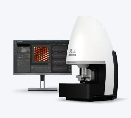
Two of the scanning probe microscopes in Dr. Piner’s care are of the very first atomic force microscopes (AFM) originating in the 1980’s from Park Scientific Instruments, a predecessor to Park Systems, both founded by Dr. Sang-il Park (Chairman and CEO). Dr. Piner acquired a Park XE-100 in 2007. Dr. Piner uses the Park AFMs on a daily basis and is one of our unique and passionate users.
Q: Dr. Piner, what is the field of your research?
Previously, we worked with synthetic graphite made of carbon-13 isotope because it has spin ½, natural carbon-12 has 0 spin. This is important since spin is needed for NMR studies of materials made from the graphite. We grew synthetic graphite on Ni foils. But we were interested in growing
thinner material and switched to copper since its ability to dissolve carbon is very low. As it happened, the first specific copper substrate we used, which we refer to as “Magic Cu”, for some unknown reason did not have any traces of chromium coating. Some copper foils have a chromium coating to prevent oxidation and keep the copper surface bright and shinny. When we ran out of that batch of copper and received a new order, suddenly we couldn’t grow graphene anymore! After scratching our heads a while, we discovered with the help of the vendor that the first batch of copper did not have chromium coating. That was the missing ingredient - and that’s the beauty of science and research discovery! The paper from that research is published and already cited around 500 times. Due to this discovery, we are now studying different effects of surface cleaning and surface preparation on the growth of graphene, which these days is a hotly pursued topic.
Q: Can you tell us about the study you are doing using an AFM?
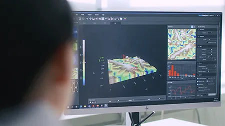
In order to use graphene for electronic purposes, it must be defect free. AFM is a really easy tool to find those small cracks or point defects that can be harder to detect with other tools. Using AFM, you can tell if you have a perfect graphene at the atomic scale. When we want to look at high detail of the graphene, we use the non-contact mode [a unique feature of Park AFM]; it is best on the Park XE-100 to get high-resolution images of the graphene structure. AFM is a nice tool to use for exploring the defects on graphene surfaces, especially using the lateral force microscopy (LFM) mode. The AFM tip is sensitive to friction, and graphene has low frictional coefficient. If you have a defect, an oxide layer will form on the copper substrate and that has a high frictional coefficient. Using the AFM, any small defect will light up like a Christmas tree!
Q: What made AFM the best choice for your study?
We have a line of instruments, AFM, SEM (scanning electron microscope), and profile meter. These cover the range of scale necessary for studying graphene in general. However, to look at the beautiful detail in the growth patterns, symmetries and snowflake structure – the Park AFMs are the best tool for that. We looked at edges of flake graphene using AFM, and we saw oxygen infiltrated under the edge of graphene. When it reached the copper substrate and oxidized, it swelled it up. When we used the SEM to see that, we kind of vaguely picked it up. However, when we used Park AFM, it was
clear as a bell. Due to the high lateral resolution of the AFM, and of course the tip sharpness, small detailed features like that can be seen using the AFM. The AFM is also beautiful to use to look at details of the fabrication process; so for example, we can look at the metal surface before and after the growth.
Q: How well is Park AFM meeting your research needs?
Pretty well so far! It has been reliable, not one mechanical failure, and the software doesn’t crash. It’s never been a problem to use Park AFM. The two older CPs from Park Scientific have been around for decades, moved around a lot and they’re still working! Let me tell you this AMAZING story about the Park XE-100. We bought the XE-100 while we were at Northwestern in Chicago but when we made the move to Austin, it was packed and
thrown into shipping crates. In the rush, I stashed the AFM head in a box – and forgot to take out the cantilever. It shipped 1200 miles over several days. In Texas, I set up the AFM and turned on the laser, and said, “Holy Cow!”.The cantilever is still there and the laser is still PRE-ALIGNED! I was mightily impressed! The AFM protected the tip and it survived the brutal move. Park should be happy and proud. Now this is what I call a reliable and well-engineered AFM.
Q: What are the key features of Park AFM do you like the most?
With the old Park Scientific AFMs, I liked the snap in and out of the tip. Actually, that feature led to the discovery of dip pen lithography.
As for the Park XE-100, I like the non-contact mode. The non-contact mode is very reliable. Basically since we have three AFMs in my lab, I dedicate each for different usage. The older Park models do the contact resistance measurement on graphene, and Park XE-100 is used for noncontact measurements. Park AFM is very nice and stable. If I put a sample in there and keep it there for a day, and come back the next day, the sample will be intact. For long-duration studies, one thing a researcher worries about is thermal stability to avoid thermal drift. The temperature stability of Park AFM is nice and consistent. Not to mention the ease of use and setting up the Park AFM.
One thing I’d like to try in the future is the conductive AFM option. It is tricky to get good images that stand out, and it does take a little effort and expertise to do so. I really would like to try the conductive AFM option on Park XE-100 when I get around to it.
Q: Which is more important to you? Accuracy vs. resolution, and vs. scan speed?
Accuracy and resolution go hand in hand. The better resolution you get with the AFM, the more accurate your result.
I’d go with accuracy vs. speed.
Published Work Using Park AFM:
Title: Mechanical Properties of Mono layer Graphene Oxide
Author(s): Suk, Ji Won; Piner, Richard D.; An, Jinho; et al.
Source: ACS NANO Volume: 4 Issue: 11 Pages: 6557-6564 DOI:
10.1021/nn101781v Published: NOV 2010
Times Cited: 30 (from Web of Science)
Title: Synthesis of graphene-based nanosheets via chemical reduction of exfoliated graphite
oxide
Author(s): Stankovich, Sasha; Dikin, Dmitriy A.; Piner, Richard D.; et al.
Source: CARBON Volume: 45 Issue: 7 Pages: 1558-1565 DOI:
10.1016/j.carbon.2007.02.034 Published: JUN 2007
Times Cited: 1,590 (from Web of Science)
Title: Atomic force microscopy study of clay nanoplatelets and their impurities
Author(s): Piner, RD; Xu, TT; Fisher, FT; et al.
Source: LANGMUIR Volume: 19 Issue: 19 Pages: 7995-8001 DOI:
10.1021/la0347814 Published: SEP 16 2003
Times Cited: 28 (from Web of Science)
Title: Cross talk between friction and height signals in atomic force microscopy
Author(s): Piner, R; Ruoff, RS
Source: REVIEW OF SCIENTIFIC INSTRUMENTS Volume: 73 Issue: 9 Pages: 3392-
3394 DOI: 10.1063/1.1499539 Published: SEP 2002
Times Cited: 23 (from Web of Science)
Title: Improved imaging of soft materials with modified AFM tips
Author(s): Piner, RD; Hong, S; Mirkin, CA
Source: LANGMUIR Volume: 15 Issue: 17 Pages: 5457-5460 DOI:
10.1021/la990408d Published: AUG 17 1999
Times Cited: 25 (from Web of Science)
Title: "Dip-pen" nanolithography
Author(s): Piner, RD; Zhu, J; Xu, F; et al.
Source: SCIENCE Volume: 283 Issue: 5402 Pages: 661-663 DOI:
10.1126/science.283.5402.661 Published: JAN 29 1999
Times Cited: 1,670 (from Web of Science)


