


Dr. Tobias Cramer,
Asst. Professor and
Researcher at Universityof Bologna, Italy.
Professor Cramer works in the semiconductor physics group at University of Bologna, Italy with a focus on flexible and stretchable semiconductors for bioelectronics and photonic applications. He teaches the course “Laboratory of Nanoscience and Technology” in the Master Degree “Materials Physics and Nanoscience (MANO)” He is responsible for the Atomic Force Microscopy lab and development of stretchable sensors for bioelectronics.
Tobias Cramer studied chemistry and physics at the University of Freiburg (D) and finished in 2006 with a Ph.D. degree. After a period of postdoctoral fellowships with stays in Germany (Institute for Advanced Studies, Freiburg), Italy (Faculty of Chemistry and Institute for the Study of Nanostructured Materials – ISMN-CNR, both Bologna) and United States (The Scripps Research Institute, San Diego). Since 2014, he has worked as a researcher in the Department of Physics and Astronomy at UNIBO, where he is a tenure track professor. In his research he investigates nano-scale charge transport phenomena in condensed matter by theoretical and experimental methods. He is the author of 45 scientific articles and book chapters.
Flexible, biocompatible electronic materials and semiconductors are wanted to create a novel generation of bioelectronic interfaces. Such interfaces will be at the heart of future medical devices that allow to record and stimulate in a low-invasive manner from the central and peripheral nervous system or to transduce directly biochemical signals. In their research they investigate in detail the material properties and the underlying physics of novel material candidates for bioelectronic interfaces. The experiments provide them the necessary knowledge to propose novel transducer concepts that could help to improve the interface between the worlds of biological cells and microelectronics.
Can you give a brief overview of Implantable Organic NanoElectronics (IONE) and describe the benefits?
In recent years materials based on organic small molecules or polymers have been developed that combine important properties of two rather different material classes: On the one hand they show semiconducting electronic properties equivalent to materials employed in modern information and communication technology. On the other hand they also have soft and biocompatible properties as well as stability in water, all typical for biomaterials. IONE employs such materials to develop novel microelectronic implants that interface to important processes in the body, relevant to diagnose or treat disease.
How are implantable organic nano electronics inspired by nature?
Information in the nervous system is processed as electronic excitations in nerve cells. The underlying microscopic mechanisms build on the cell’s ability to control tiny ionic current fluxes. The immense relevance of ion transport processes in Nature stimulates the research done for IONE. Modern information and communication technology materials control electronic excitations and currents in a very precise way, but ionic mechanisms do not play any role. IONE is changing this paradigm and some novel organic materials show efficient ionic as well as electronic transport. This opens also new opportunities to build improved bioelectronic interfaces.
How are IONE different from bioelectronics?
IONE is developing new means to perform bioelectronic research or to interface to bioelectronic systems. With the help of organic nanomaterials less invasive interfaces are developed that permit a two-directional communication with the neuronal system. Recording with such interfaces will allow us to intercept the body’s communication channels. Stimulation instead allows us to impact on them
Can you explain how they can be used in Human Technology interfaces and give some examples?
The materials that we are investigating are designed to build less invasive interfaces with the nervous system that could operate in chronic conditions. That means during normal activity the IONE microdevices are able to record signals from the body and analyse them continuously without interference or impact on the body’s own processes. Such a recording technology will help to increase our knowledge about the bioelectronic signaling processes in the human body in a much more precise way. For example, there is currently only a rough understanding that the peripheral nervous system is also responsible for immune response and inflammation. A precise understanding and then the possibility to impact on the related signals by stimulation could provide new means to treat disease states locally and without pharmaceuticals.
Can you describe the latest discovery of Direct electrical neurostimulation with organic pigment photocapacitors and why this is important research?
This research regards an organic nanomaterial that has been invented by Eric Daniel Glowacki at Linköping University. As Physicists we investigate in detail the microscopic mechanism that occurs when such materials are illuminated by a strong red light source. And it is remarkable. Although it consists of a layer of only a few tens of nanometers, it leads to the efficient generation of a charged bilayer. The resulting transient ionic current pulse is sufficiently strong to excite neuronal cells. So this material is becoming a very hot candidate for artificial retina implants. With this device no battery support or wiring with cables will be necessary. The light pulse will provide enough energy to excite the visual nerve locally, potentially making such implants much more simple and less invasive.
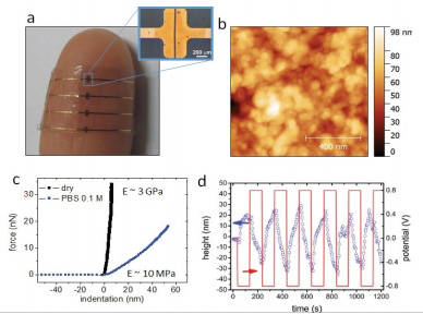
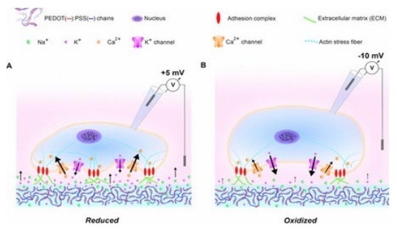
Left: Soft conducting polymer based bioelectronic interfaces: (a) Flexible, biodegradable interface to measure ECG signals; (b,c,d ) investigation of morphology, mechanical properties and electroactuation of conducting polymer thin film (Pedot:Pss) in water with AFM methods.
Can you describe the potential for use in space environments to reduce damage from ionizing radiation?
This relates to a different class of semiconducting materials that we are investigating in our lab. For the space environment we need semiconductors that show an enormous chemical and structural stability. The problem is that in space, everything is subjected to large amounts of ionizing radiation. Organic electronics for example seems to degrade earlier under such conditions. So for that purpose we investigated amorphous oxide based semiconductors. Similar to organic materials amorphous oxides can be patterned on large areas and on flexible substrates leading to bendable, large area electronic devices. Now for the space environment, oxide electronics have the big advantage that they are highly resistant to ionizing radiation as we demonstrated with our research work
How is AFM used in your research?
We have many different applications for AFM. In fabrication work we use it a lot in routine investigations of surface morphology and layer thickness. But what I like about AFM is its versatility. Multimodal techniques provide much more information than just morphology. For the research of novel electronic materials this is fundamental. For example with KPFM we can measure now in detail how the electronic transport properties of our semiconducting layers vary while we start to apply tensile strain to the material and stretch it.
What other advances do you see in the field of IONE? Give some future predictions.
First of all, we still have to focus our efforts to bring organic nanomaterials to real clinical applications. Currently we have demonstrated impressing proof of principles, but to push these concepts forward into real improvements for patients will take more energy. Then of course also for the future I can imagine some promising developments for organic nanoelectronics. Of course our dream is to extent technological information processing into 3D by using our novel materials, but that is another story …
You are teaching a course called, "LABORATORY OF NANOSCIENCE AND NANOTECHNOLOGY". Do you think students today view science drastically differently, compared to students who studied science before the Nanotechnology boom in the 1980s?
Yes of course it is different and that is the reason why we recently introduced the new master course “Materials Physics and Nanoscience” at our University in Bologna. At first sight one would think that students just have to learn more and more, but I think this is not the case. Focus has to be set on important concepts and one also has to take experimental skills seriously. Regarding the recent developments in equipment it has also become easier to teach nanoscience. For example nowadays it is no problem that students perform their own AFM experiments independently in the laboratory course.
What Students Say about the course:
“I didn’t expect to work on my own with an AFM in a laboratory course. It helped me a lot to figure out how AFM works in practice and it was very motivating.” Matteo Verdi, MANO student, University of Bologna 2018
“The laboratory of nanoscience and technology course was fantastic: it provided us with the basic knowledge about nanoscience. We also had a lot of opportunities to get into contact with real research problems.” Giovanni Armaroli, MANO student, University of Bologna 2018
In our group we employ a Park NX10 AFM equipped with different modules allowing for multimodal AFM techniques.
Soft bioelectronic devices that interface non-invasively neuronal tissue are expected to open an enormous potential for novel medical therapies.
This technology encounters a fundamental limit as a compromise between mechanical stability and the medical invasiveness has to be found: Bioelectronics interfaces should match the soft
elastic properties of the tissue where they are embedded (E < 1 MPa). Missing compliance with the low elastic modulus of tissue leads on the long-term to inflammation, scar formation and passivation. However, bio-electronic implants rely on patterned microelectronic structures made of more rigid electronic materials for signal recording and stimulation. The resulting mismatch in mechanical properties imposed by the requirement of a soft substrate combined with electrical functional rigid elements makes bio-electronic microelectrodes prone to stress induced mechanical failure and does not allow any further miniaturization and reduction in invasiveness.
To overcome the fundamental limitations in the engineering of soft, multi-component microelectronic devices, Dr. Cramer’s group investigates novel materials and device architectures that combine soft mechanical behaviour with stable electronic performance. They employ a wide range of macroscopic and microscopic techniquecs to decipher the combined electromechanical effects relevant for bioelectronic interfaces.
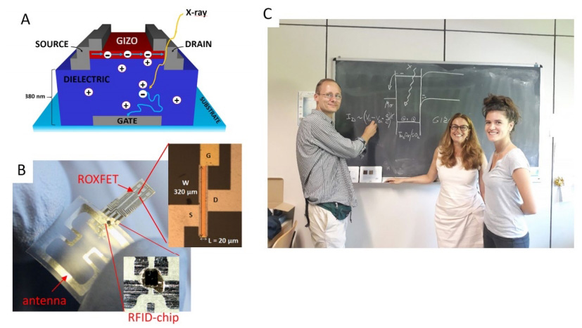
Figure: Novel microelectronic X-ray dosimeter compatible with flexible plastic substrates and passive RFID detection A) Scheme showing the operation mechanism of the dosimeter that employs a radiation sensitive oxide field effect transistors (ROXFET) B) Photo showing the wireless RFID sensor. The insets show micrographs of the RFID chip and of the ROXFET microelectronic dosimeter. C) Photo of the UNIBO team working on the project (from left to right: Tobias Cramer, Beatrice Fraboni, IlariaFratelli).
Wireless, flexible, low-power and realtime microelectronic X-ray dosimeters
Authors and affiliations: Tobias Cramer*, Ilaria Fratelli1 , Pedro Barquinha2 , Ana Santa2 , Cristina Fernandes2 , Franck D’Annunzio3 , Christophe Loussert3 , Rodrigo Martins2 , Elvira Fortunato2 , Beatrice Fraboni1
1. Department of Physics and Astronomy, University of Bologna, VialeBertiPichat 6/2, 40129 Bologna, Italy.
2. CENIMAT/I3N and CEMOP-UNINOVA, Departamento de Ciência dos Materiais, Faculdade de Ciências e Tecnologia, Universidade NOVA de Lisboa, Campus de Caparica, 2829-516 Caparica, Portugal.
3. Tagsys Rfid, 785 Voie Antiope, 13600 La Ciotat, France.
Introduction: Exposure to ionizing radiation such as x-rays or γ-rays may alter the atomic and molecular structure of materials and biological compounds representing a threat to human health as well as to electronic devices, as the modifications induces by irradiation can cause cancer in humans or failure in devices. To avoid health or technical safety risks the exposure to ionizing radiation has to be tightly controlled in a wide range of applications that span from medical radiotherapy and nuclear waste management to high energy physics experiments and space missions. .Currently available radiation dosimeters that provide information in real-time are designed as high precision devices, but are often expensive and with rather large and bulky shapes. In order to continuously monitor radiation exposure, low-cost and non-invasive microelectronic dosimeters are highly wanted. Traditional microelectronic materials such as crystalline silicon cannot easily meet the application requirements of microelectronic dosimeters for two reasons: First, they do not absorb sufficient amounts of high energy radiation to be sensitive as they contain mostly elements with a rather low or medium atomic number Z. Second, as crystalline materials, they are fabricated on rigid wavers and cannot be patterned onto flexible plastic foils.
Results: In order to overcome these limitations our research team has been investigating amorphous oxide semiconductors as novel materials for microelectronic dosimeters. Oxide semiconductors based on Indium Gallium Zink Oxide (IGZO) have the right structural and electronic properties to achieve fast transport of electrons as a n-type semiconductor even in the case of an amorphous, that is disordered, microstructure. This opens the way to deposit the IGZO semiconductor by physical methods on large flexible substrates instead of relying on crystalline growth. For our research on microelectronic dosimeters, we combined the IGZO transistors with a high-Z oxide dielectric that absorbs the ionizing radiation and builds up a space charge layer. The combined device structure, that we call radiation sensitive oxide field effect transistor (ROXFET), is shown in Figure 1. By introducing the amorphous oxide based semiconductor, we achieve a microelectronic dosimeter that outperforms similar silicon based devices by an order of magnitude in sensitivity achieving the detection of radiation doses down to the 100 µGy range. In addition, we demonstrate that the dosimeter can be patterned in arrays on flexible plastic foil. The fast electronic transport properties of IGZO make it also possible to integrate the ROXFET in a passive RFID circuit. With support from the French company Tagsys-RFID we created the first wireless radiation sensor that is operated without a battery. Its detection mechanism is so energy efficient, that a radio frequency signal as generated by an RFID reader provides enough energy to operate the sensor and to send back to the reader the information on the sensor irradiation status.
The research has been carried out in collaboration with the group of Prof. Rodrigo Martins of the Universidade Nova di Lisbon (PT) and the results have been recently patented and published in Science Advances.Our results pave the way towards a new generation of flexible, real-time and low-power microelectronic dosimeters able to provide continuous, non-invasive and fully passive monitoring of ionizing irradiation exposure, e.g. during medical radiotherapy or during space mission to monitor exposure during radiotherapy or radiation damage in electronics. To find full article go to: http://advances.sciencemag.org/ content/4/6/eaat1825


