


Changing the Future of Nanometrology for the Semiconductor Industry
Abstract
The Three-Dimensional Atomic Force Microscopy (3D AFM) by Park Systems is an innovative and cost effective means of accurately characterizing the roughness and the sidewall morphology of photoresist semiconductors and was created by industry’s need for a nanoscale measurement tool that surpassed the limited scans available using SEM. As the device critical dimension decreased, industry demanded an advanced method for high resolution data. The 3D AFM offers a unique solution to the challenges facing semiconductor manufacturers and provides many cost effective and resolution advantages not previously available in standard systems. One of the most unique features of Park 3D AFM is the independent Z-scanner that can be tilted in order to gain access to the sidewalls of the material and, hence, measure its critical dimensions (CD), its sidewall and line edge roughness (SWR and LER respectively). This article will briefly introduce the notions behind the Park 3D AFM and will demonstrate its capability to acquire high-resolution measurements of both sidewall and line width roughness (LWR) throughout the pattern transfer process. Another feature highlighted is the unique low noise level properties that are of utmost significance when dealing with metrology tools. Finally, by varying the aerial image contrast (AIC), different degrees are derived of line edge roughness identifying trends in sidewall-roughness that clearly depend on the levels of AIC.
Introduction
One of the most challenging features in the semiconductor industry is the continuous research and the subsequent fabrication of integrated circuits with enduringly smaller critical dimensions (CD). This term not only defines the respective smallest possible feature size of the semiconductor itself but it is also interwoven with the design and implementation of a viable, refined, easy–touse and accurate apparatus that will allow for measuring various parameters such as the line edge roughness (LER), the line width roughness (LWR) and the sidewall roughness (SWR). The characterization of such factors that determine the shape and the roughness of the device patterns for device manufacturers is of utmost importance due to the fact that they directly affect the device performance. Optical lithography, which was initially used for the creation of patterns in the manufacturing of semiconductors, is severely limited in terms of resolution. Therefore, the existing prevalent method for measuring these factors prior to 3D AFM was primarily the scanning electron microscopy (SEM) with its image analysis software. Despite the fact that this technique offers substantial advantages such as automation and compatibility with standard critical dimension SEM tools, it cannot provide the user with high resolution LER data due to the fact that SEM resolution is reaching its limits, therefore 3D AFM offers a highly desirable solution. Leading manufacturers have implemented Park 3D AFM that can measure resist profile, LER and SWR in a way that is highly accurate, non-destructive and costeffective. The precise and full characterization of such features is extremely essential during the pattern transfer process as it offers the possibility of imaging all surfaces of the pattern.
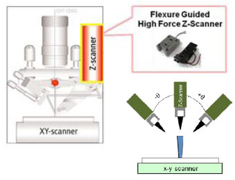
What is non–contact 3D AFM and what are its innovative features?
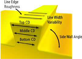
The basic principle of non-contact 3D-AFM is that the cantilever rapidly oscillates just above the surface of the imaging sample. This offers a plethora of advantages, as compared to the traditional contact and intermittent modes. One of the most essential advantages is that there is no physical contact between the tip and the surface of the sample. Moreover, as depicted in figure 2, the Z-scanner, which moves the tip, is decoupled from the XY scanner, which solely moves the sample, thus, offering incredibly flat scanning and an additional benefit by improving its Z-scan bandwidth. Furthermore, by tilting the Z-scanner we can access the sidewall of the nanostructures and perform roughness measurements along the sidewall of photoresist lines while at the same time measure the critical dimensions of top, middle, and bottom lines (see figure 2).
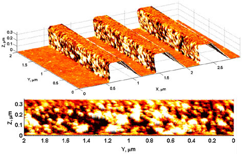
More specifically, data acquisition is performed by a conical tip in predefined tilted angles typically 0º, a, and -aº. Consequently, and by combining these three scans (a method called image stitching),we can reconstruct the 3D pattern as shown in figure 3.
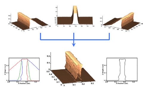
This provides an excellent and extremely accurate method that takes advantage of the interference pattern of the standing waves in order to measure features such as the total height, the top, middle, and bottom width. This system is capable of advanced threedimensional imaging of both isolated, and dense line profiles. AFM is less costly than the alternative techniques (CD-SEM and focused ion beam (FIB)) for imaging and measuring parameters of line profiles since the preparation of the sample is by far simpler.
Noise levels in 3D-AFM
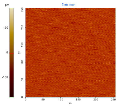
A critical requirement when dealing with metrology tools is associated with constraining the level of noise in the manufacturing environment, which Park has studied and researched extensively, providing evidence that correlates noise levels with productivity. The study of noise levels on a 300 mm wafer proved that Park 3D-AFM is not only a powerful nanocharacterization automated tool with excellent resolution but also a system that keeps the overall system noise at levels lower than 0.05 nm (0.5 angstrom) as depicted in figure 4.
Roughness Measurements
Roughness can be transferred into the final etched profile, thus, roughness measurements can describe and determine the quality of the patterns. The unique tilted Z scanner in combination with the low noise levels that are prevalent during the AFM process can provide excellent and very accurate results in terms of sidewall roughness measurements. Figure 5 depicts the 3D AFM imaging of a photoresist semi-dense line pattern and the respective grainy structure of its sidewall. The precision with which the SWR was measured is validated by the excellent repeatability (0.08nm 1 sigma for 5 sites wafer mean) for the sidewall roughness of about 6.0 nm.
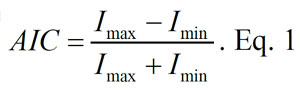
It needs to be noted that roughness depends, amongst others, on the aerial image contrast (AIC) or in other words the physics of exposure. AIC is determined as the quotient between the subtraction and the addition of the maximum and minimum image intensities.
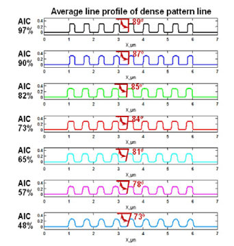
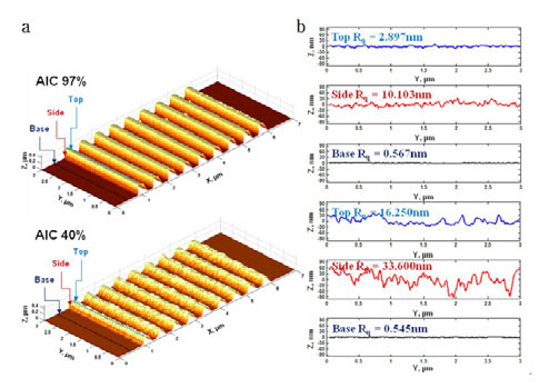
Several consequent series of images with variable exposure reveal that LER significantly increases when the AIC is decreased, a fact that underlines that AIC is a controlling factor for LER. Moreover, and as depicted in figure 6, reduced levels of AIC produced line profile images of the resist that were more blunted, and also smaller sidewall angles (SWA). Figure 7 illustrates the capability of Park 3D AFM to image all surfaces of the pattern, in contrast to the conventional AFM or the SEM, which cannot fully characterize the surface data, and obtain information such as base, top and both sidewall roughness from sidewall characterization. We imaged a 300 nm photoresist line pattern and we obtained the respective line profiles that clearly showed a substantial difference in terms of SWR between 97% and 40% AIC. More specifically, the lower the value of AIC the more increased was the measured roughness. This intense decrease of roughness is underlying the fact that LER and the measured sidewall roughness are clearly correlated.
Finally, it needs to be emphasized the role of non-contact 3D AFM in terms of preserving the tip sharpness of the cantilever. In an independent study, researchers performed 150 consecutive measurements using the same tip and the tip wearing proved to be minimal. This is a prominent feature of AFM that prevents the continuous costly replacement of the tip but also ensures that the sample will be viable and not damaged by the AFM cantilever. The preservation of the tip sharpness allows for continual measurements of high resolution roughness data.
Conclusions
This paper clearly demonstrates the potentialities of the innovative, nondestructive imaging technique of 3D AFM compared to the existing SEM system. Clear examples of the many features of 3D AFM include the introduction of an independent and tilted Z-scanner proven to overcome the disadvantages of alternative metrology tools and measure parameters such as detailed sidewall morphology and roughness, and sidewall angle characterization that render the optimization and evaluation process easier and far more detailed. The development of 3D AFM by Park Systems proves to keep pace with the requirements and challenges from continuously shrinking semiconductor device critical dimensions by offering a solution that encompasses excellent resolution, high precision and accuracy, and easy sample preparation. 3D AFM sets a new standard for nanotechnology measurement and performance in a rapidly changing industry where new technologies and advancements pioneer future opportunities. About Park Systems Park Systems is a leading manufacturer of atomic force microscopy (AFM) systems with a complete range of products for researchers and industry engineers in materials science, chemistry, physics, life sciences, semiconductor and data storage industries. Park’s products are used by over a thousand of institutions worldwide. Park’s AFM features unique patented set of technologies that yields highest data accuracy at nanoscale resolution, superior productivity, and lowest operating cost to its customers. Park Systems, Inc. is headquartered in Santa Clara, California with its global manufacturing, and R&D headquarters in Korea. Park’s products are sold and supported worldwide with regional headquarters in the US, Korea, Japan, and Singapore, and distribution partners throughout Europe, Asia, and America. Please visit www.parkafm.com or call 408-986-1110 for more information.


