Park Systems, the enabler of nanoscale advances, invites you to discover an exhibition that will immerse you in the most sophisticated nanotechnology. Please visit our booth at SEMICON West 2014 being held at the Moscone Center in San Francisco.
l Date : July 8 – 10, 2014
l Venue : Moscone Center – San Francisco, CA (United States)
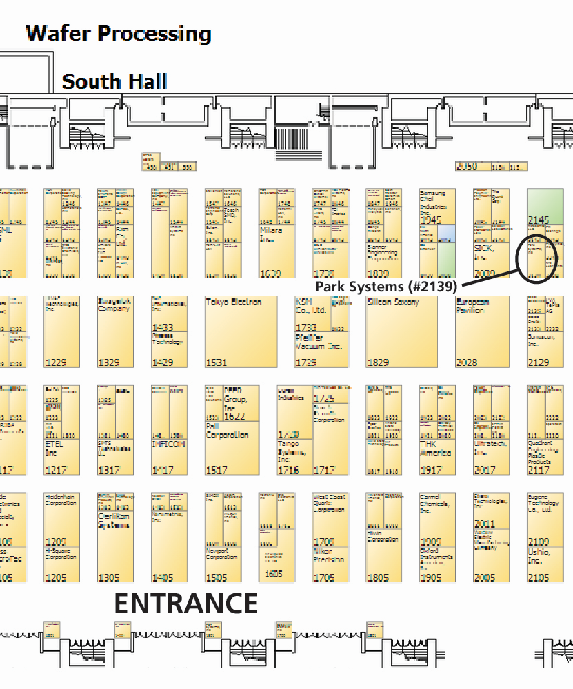
l Park’s Booth : South Hall, No. #2139
Remember to also join our SEMICON West 2014 AFM Luncheon and Reception at the nearby Jillian's, just a short walk from the Moscone Center:

l Date : July 9, 2014
l Venue : Jillian's (click for directions from the Moscone Center)
l Attending? Make sure to register yourself and/or your group online.

*EVENT OPEN TO RESEARCH ACADEMIA AND INDUSTRY PROFESSIONALS ONLY; REGISTRATION WILL BE SCREENED. ONLY COMPANY/UNIVERSITY EMAIL ADDRESSES WILL BE ACCEPTED.
Park Systems is proud to announce that we will be hosting Phil Kaszuba, Advisory Engineer to the Scanning Probe Microscopy (SPM) Laboratory of the IBM System and Technology Group in Vermont. Phil will be presenting "The Role of Scanning Probe Microscopy in Nanoscale Semiconductor Device Analysis":

Phil Kaszuba
Advisory Engineer
Scanning Probe Microscopy (SPM) Laboratory
IBM System and Technology Group
ABSTRACT:
Since the invention of the Atomic Force Microscope (AFM) in 1986, numerous analytical techniques have been developed and implemented on the AFM platform, evolving into what is collectively called the Scanning Probe Microscope (SPM). The SPM has since become established as a mainstream analytical instrument with a continually increasing role in the development of nanoscale semiconductor technologies providing critical data from initial concept to technology development to manufacturing to failure analysis. This presentation will discuss Atomic Force Microscopy (AFM), Scanning Kelvin Probe Microscopy (SKPM), Scanning Capacitance Microscopy (SCM), Conductive-AFM (C-AFM), Magnetic Force Microscopy (MFM), and Scanning Surface Photo Voltage Microscopy (SSPVM). An overview of each technique will be presented along with examples of how each is currently used in the development of new technologies, the monitoring of a manufacturing line, and the failure analysis of nanoscale semiconductor devices.
Following Phil's presentation, Dr. Ardavan Zandiatashbar of Park Systems will present the following topic: "Smart Automatic Defect Review (ADR) for 300 mm bare wafers: a preventive approach for quality assurance in semiconductor manufacturing":
ABSTRACT:
Wand controlling the cost of IC manufacturing. AFM has been already proven to be a unique non-destructive technique for providing accurate three-dimensional information on the defects (without leaving irradiation marks like SEM). However it was limited due to its throughput, and laborious efforts for finding the defects. Park Systems recently introduced its unique solution for 300 mm wafer technology: the smart Automatic Defect Review (ADR), on Park's Wafer series. In this talk, ADR's capabilities will be discussed and presented along with examples of ADR on 300 mm bare silicon wafers. With the help of Park's Smart ADR, the throughput for defect review using AFM tools has been improved by 1000%. hile the semiconductor industry is concentrating more on sub-45 nm nodes and larger incoming wafers, defect inspection and review is playing a key role in increasing the yield
About SEMICON West :
Founded 1971 (2014: 44th year)
SEMICON West is the flagship annual event for the global microelectronics industry. It is the premier event for the display of new products and technologies for microelectronics design and manufacturing, featuring technologies from across the microelectronics supply chain, from electronic design automation, to device fabrication (wafer processing), to final manufacturing (assembly, packaging, and test). More than semiconductors, SEMICON West is also showcase for emerging markets and technologies born from the microelectronics industry, including micro-electromechanical systems (MEMS), photovoltaics (PV), flexible electronics and displays, nano-electronics, solid state lighting (LEDs), and related technologies.
l Link : http://www.semiconwest.org/
Exhibit Floor Plan