


Introduction and Sample Description
Because of its ferromagnetic properties with well-oriented interfaces at room temperature, epitaxially grown MnAs film on GaAs substrate is one of the most promising systems for future spintronic applications despite the large lattice mismatch between the epitaxial film and its substrate material. The bulk MnAs shows a phase transition from the ferromagnetic (FM) α-MnAs to the paramagnetic orthorhombic β-MnAs at the critical temperature of about 45 °C.3 In the MnAs thin film systems, the two phases coexist in the form of self-organized periodic stripes at room temperature, occurring via strain stabilization. The periodic length of the two coexisting phase stripes depends strongly on the film thickness. In this note, MnAs films with varying thickness are observed in various magnetization states.
The MnAs films investigated herein were grown on GaAs(001) substrates at 270 °C by molecular beam epitaxy with varying thickness of 10, 20, 50, 100, 250, and 500 nm, respectively. At room temperature the strain-stabilized coexistence of the two phases was confirmed by X-ray diffraction experiments. By using a superconducting quantum interface device magnetometer (SQUID) the magnetic properties were also investigated. Also, Atomic Force Microscopy (AFM) and Magnetic Force Microscopy (MFM) data show that the α-MnAs and β-MnAs stripes are aligned along the MnAs[0001] and perpendicular to the magnetic easy axis MnAs[1120].
The MFM images were acquired by using a Park AFM with MFM option and a magnetic cantilever (Nanosensors). A magnetic field generator was used to apply magnetic field to the samples, which generates magnetic fields up to 600 Oe.
Experimental Details
For the characterization of magnetic samples such as epitaxially grown MnAs films, measurement of their local magnetic property is crucial. Though SQUID gives quantitative magnetic data about the sample under investigation, the lack of spatial resolution does not give structural analysis regarding the material. MFM data, on the contrary, reveals local magnetic properties of the samples along with well-defined topographic data.
A vital requirement for these precise measurements by MFM is the explicit separation of the magnetic signal from the topographic data. While the MFM signal is collected from the instrument, the cantilever is positioned at a certain distance from the sample surface, so that the van-der-Waals force do not interfere the magnetic force. To maintain this condition, the position of the cantilever is controlled very accurately. In conventional piezoelectric tube based AFM systems, the Z direction movement (which corresponds to the height data) is coupled with the XY direction scanner movement due to its geometrical design limitation. The crosstalk between XY and Z movement introduces topographic error signal to the magnetic signal, and it needs accurate and stable calibration to obtain realistic results. On the contrary, Park AFM introduces a perfectly decoupled XY and Z-scanners to prevent the interference of the movement crosstalk. The separated movement of Park AFM secures the real MFM data which is decoupled from the topographic signal.
Data Analysis
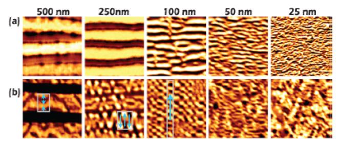
Figure 1. MFM images of epitaxially grown MnAs films with various film thicknesses of 500 nm, 250 nm, 100 nm, 50 nm, and 25 nm, respectively at (a) the saturated state and (b) the demagnetized state. Observed area is 5 μm in each direction, and the magnetic easy axis of each film is perpendicular to the FM stripes.
Figure 1 shows the MFM images of the MnAs films with various thicknesses of 25 nm, 50 nm, 100 nm, 250 nm, and 500 nm, respectively, at (a) saturated state and (b) demagnetized state. In these images, the easy axis of each film is perpendicular to the stripe direction, and the observed area is 5 μm in each direction. As shown in Figure 1(a), all the ferromagnetic (FM) stripes in each saturated film are in a single domain state, where MFM contrast in each stripe is ascribed to the stray field from the boundary between the neighboring stripes. Also it is observed that the periodic length and the widths of the α and β phase stripes decrease as the film thickness decreases, which correlates well with strain relaxation effects.
In Figure 1(b), change in the domain structure of the demagnetized films is observed, as the film thickness decreases. In the image of the 500-nm-thick sample, the domain structure within the FM stripes can be described as head-on domains, which are expressed as the spin configurations in which the magnetization directions of two domains meet head-on as demonstrated in the rectangular box of the MFM images. In the image of 250-nm-thick sample, two kinds of domain structures are observed, head-on domains and simple domains. The simple domains are defined as the spin configurations having a single spin direction along the width of the FM stripe, as demonstrated in the rectangular box of the MFM image. The existence of head-on domains in 250 and 500-nm-thick samples indicates the formation of a closed domain configuration inside the film, which is expected considering that the domain wall length of the MnAs film is about 100 nm.9 Also, the simple domains in the films whose thicknesses are less than 100 nm appear because the film thickness is less than the domain wall length.
When the film thickness is less than 100 nm, the correlation between the spin directions in the domains of the neighboring FM stripes becomes significant. In the MFM image of the demagnetized 100-nm-thick sample, the stripes in the rectangular box indicate that the spin directions of the stripes are aligned in the same direction due to the dipolar interactions between the neighboring stripes.
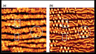
Figure 2. (a) AFM and (b) MFM image of the 250-nm-thick MnAs film on an area with a large fluctuation in the FM stripe width.
Especially, in the image of the demagnetized 250-nm-thick sample, the two types of domain structures are found despite of its uniform thickness. This indicates that there may be another major origin for the change of the domain structure in the FM stripe in addition to the film thickness. For further understanding, the AFM and MFM images of the 250-nm-thick MnAs film were investigated on the area with a large fluctuation in the stripe width, as in Figures 2(a) and (b). In these images, simple domains are observed where the width of stripes is relatively narrow, whereas the head-on domains appear where the width is relatively wide. This can be explained by the difference in the demagnetizing factor, which can be estimated by width over thickness (w/t) stripes ratio. From the images shown in Figure 1(b), the w/t ratio of the 500-nm-thick sample is 3.1±0.1, whereas 5.8±2.0 is measured for the 100-nm-thick sample. Considering this, the change of the domain structure from the head-on domain to the simple domain can be ascribed to the increase in the demagnetizing factor which is due to the change in the stripe width as well as in the film thickness. In Figure 2(b), the simple domain structure is observed where the width of the stripe is relatively wide. On the other hand, the head-on domain structure is observed where the width is relatively narrow.
The demagnetizing factor also can be influenced by the change in the gap distance between the stripes. As shown in the circular box of the Figure 2(b), the estimated demagnetizing factor of this area is 4.0, which is lower than the average demagnetizing factor of the FM stripes in the film, 4.7±1.3. This indicates that the increased dipolar interaction between neighboring stripes due to the narrow gap induces a simple domain structure despite the small w/t ratio in this particular area.
References
1. G. A. Prinz, Science 250, 1094 (1990).
2. M. Tanaka et al., Appl. Phys. Lett. 65, 1964 (1994); A. Trampert et al., ibid. 79, 2461 (2001).
3. N. Menyuk et al, Phys. Rev. 177, 942 (1969).
4. V. M. Kaganer et al, Phys. Rev. Lett. 85, 241 (2000); Phys. Rev. B 66, 045305 (2002).
5. T. Plake et al, Appl. Phys. Lett. 80, 2523 (2002).
6. L. Däweritz et al, J. Appl. Phys. 96, 5056 (2004).
7. K. Ryu et al., Phys. Rev. B 71, 155308 (2005).
8. K. Ryu et al., Appl. Phys. Lett. 89, 232506 (2006).
9. F. Schippan et al, J. Appl. Phys. 88, 2766 (2000).
Courtesy
This note is based on the data kindly provided by Prof. Young Pak Lee, Quantum photonic science research center, Hanyang University, which is published in the article, Applied Physics Letters 89, 232506 (2006).


