


Park AFM instruments create new ways to understand GaN HEMT reliability issues
Case Study: AlGaN/GaN HEMT reliabilityBy Chung-Han Lin, D. R. Doutt, and L. J. Brillson
General considerations
AlGaN/GaN high electron mobility transistors (HEMTs) are promising devices for future high power and high speed application due to their high breakdown voltage, high current density, and high temperature capability1. However, high voltage and current generate large piezoelectric stress2 and high temperature3, challenging our understanding of AlGaN/GaN HEMT device reliability and device failure. High temperature generated inside the operating device combines with other effects such as field-induced mechanical stress, occurs in different localized areas and makes device failure difficult to understand and predict.
Park AFM System Overview
At the core of our nanoscale measurements is the Park AFM system with the Enhanced EFM module. The high lateral resolution allows for investigating highly localized failure regions with small device dimensions. Coupled with KPFM potential maps and depth-resolved cathodoluminescence spectroscopy (DRCLS), this allows for accurate investigation of defect generation or even failure mechanisms of AlGaN/GaN HEMTs. Furthermore, the True Non-Contact mode successfully maintains the tip-sample distance of only a few nanometers allowing for measurements that do not disrupt the surface or its features. This capability is vital for obtaining accurate electronic and morphological information near subsurface defects.
Surface potential evolution of AlGaN/GaN HEMT under stress
We have already shown that the Park AFM system has excellent spatial resolution for investigating ZnO nanostructures.4 Here we use the Park atomic force microscopy (AFM) with Kelvin probe force microscopy (KPFM) capability and DRCLS to investigate the reliability issues of start-of-the-art AlGaN/GaN HEMT under off-state (high voltage, low current) stress. With this nanoscale technique, we are able to measure both where and how electric-field-induced stress degrades AlGaN/GaN HEMTs, and the electrically-active defects produced at local degradation areas, thereby allowing us to predict where device failure will occur.
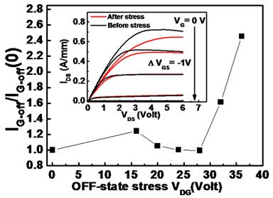
Figure 1. DC output characteristics and IG-OFF as a function of Off-state stress VDS = 10 – 30 V and VGS = -6 V. Inset shows DC-IV characteristics before and after stress.[5]
Figure 1 shows DC-IV and IG-OFF before and after OFF-state stress. Gate leakage current (IG-OFF) increases by 2.6x with VDG, rising sharply above a 28 V critical voltage after Off-state stress. The decrease of the drain current (IDS) and the increase of IG-OFF indicate the deterioration of device performance due to off-state stress.
With increasing Off-state stress, KPFM reveals micron-scale patches of lower potential/Fermi level (EF). Figures 2 display the KPFM and AFM results, of gate (G), drain (D), and source (S) at two representative area of a AlGaN/GaN HEMT without surface passivation. The region between G & D and G & S is defined as extrinsic drain and source, respectively. The KPFM images show a striking evolution of surface potential with increasing stress voltage VDS as low surface potential patches begin to grow. Initially, the lowest potential area extends along and on both sides of the gate. Between VDG = 24 and 32 V, the lowest potential area shifts to the gate edge on the drain side. As VDG increases further, this lowest potential area (marked as black-dashed circle) expands and extends from the gate edge across the extrinsic drain region. The surface potential at this extended area decreases from ~ 0.4 V to -1.6 V. AFM shows no surface morphology changes during these potential changes from the rectangular gate edge to the drain.
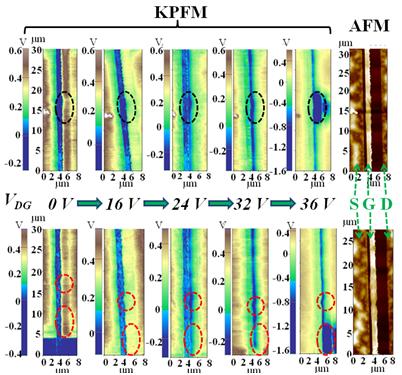
Figure 2. KPFM results which shows the evolution of surface potential under Off-state stress at two representative areas of AlGaN/GaN HEMTs. AFM images show the topography results of these two representative areas at VDG = 36 V. The dashed circles show regions where potentials change faster.[5]
Increasing Off-state VDS further results in a broken gate, a crater forming at 15 µm away from the beginning of the extrinsic drain region, and thus device failure. Images obtained by scanning electron microscope (SEM) system before and after off-state stress were shown in figure 3. Correlating the potential and morphology results versus electrical stress, one can link device failure with lower surface potential area. As stress voltage increases, device properties gradually degrade toward failure - faster for VDG above a ~28 V critical voltage. Although no AFM or SEM morphology changes can be observed before device fail, surface potential changes dramatically with stress. Furthermore, failure occurs close to the region of lowest potential. Failure is defined here as a crater in the extrinsic drain region. Likewise, the lower the surface potential, the more probable failure occurs there. Therefore, surface potential appears to be a strong indicator for device failure: (i) low potential (e.g., decreasing by > 1.5 eV) patches indicate likely failure points, (ii) a patch with the lowest potential is likely the initial point of failure, (iii) the lower the potential, the closer to device failure.
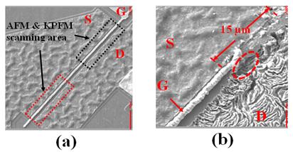
Figure 3. The SEM image indicates where failure occurs with increasing Off-state stress. (a) whole device, and (b) enlarge view of black rectangle in (a) after device failure occurs. [5]
DRCLS result at one of the lowest surface potential areas (point 9 in figure 4) in the extrinsic drain region after Off-state stress not only show the 3.45 eV near band edge emission (NBE), but also a 2.2 eV yellow band (YB) and 2.8 – 3.0 eV blue band (BB) are evident. Figure 4 also shows that the surface potential correlated with the YB/NBE ratio very well, i.e. the lower the surface potential, the higher the YB/NBE ratio. The formation of the low surface potential patches was caused by the generation of electrically-active defects due to field-induced stress VDS. These defects will move the EF position and thus affect the surface potential which can be detected by KPFM technique. A more complete analysis and detail explanation can be found elsewhere5.
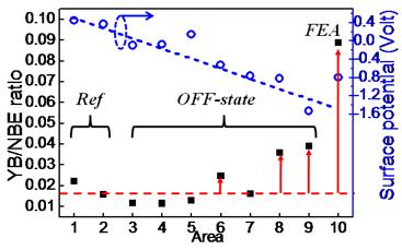
Figure 4. Surface potential and average YB/NBE intensity ratio increases with Off-state stress. YB/NBE increases most at lower potential regions 6, 8, 9, and 10. Higher potential patches display slower changes. 1 and 2 correspond to extrinsic drain and drain-side gate edge of an unstressed reference device.[5]
Conclusion
The ability to simultaneously image topographical and electronic properties on the nanometer scale is not only a highly powerful technique for understanding the basic physics of materials, but it is also is very useful in examining device structures and their failure mechanisms. Here, we demonstrate the failure-related surface potential evolution with increasing off-state stress on a nanometer scale. The low potential patches appear and then expand at extrinsic drain region indicate where electrically-active defects grow, and where device failure occurs. The lowest surface potential region is likely the device failure occurs due to highest defect density. With superior sensitivity and spatial resolution, the Park AFM/KPFM can be used to investigate device reliability issues without time consuming lifetime tests.
Note
This work is supported by the Office of Naval Research Grant No. N00014-08-1-0655 (Dr. Paul Maki and Harry Dietrich)
Reference
1Y. F. Wu, D. Kapolnek, J. P. Ibbetson, P. Parikh, B. P. Keller, and U. K. Mishra, IEEE Trans. Electron Dev., 48, 586 (2001)
2J. A. del Alamo and J. Joh, Microelectron Reliab., 49, 1200 (2009)
3C.-H. Lin, T. A. Merz, D. R. Doutt, M. J. Hetzer, J. Joh, J. A. del Alamo, U. K. Mishra, and L. J. Brillson, Appl. Phys. Lett., 95, 033510 (2009)
4T. A. Merz, D.R. Doutt, T. Bolton, Y. Dong, and L.J. Brillson, Surface Science (Letters), 605, L20 (2011)
5C.-H. Lin, D. R. Doutt, U. K. Mishra, T. A. Merz, and L. J. Brillson, Appl. Phys. Lett., 97, 223502-1 (2010)


