


As the dimensions of semiconductor devices continue to decrease, their electrical and chemical characterization becomes a challenging task for device engineers and researchers. Standard methods for characterizing semiconductors like Secondary ion mass spectroscopy (SIMS), Spreading resistance profiling (SRP), and one-dimensional capacitance-voltage (C-V), etc. do not provide an effective means to determine functional properties on sub-device scale. To achieve a sufficient resolution for the continuous reduction of device dimensions and to meet high reliability demands required for their characterizations, various types of Scanning probe microscopy (SPM) have been applied to image devices and monitor electronic processes. In particular, Scanning capacitance microscopy (SCM) is a powerful atomic force microscopy (AFM) method for the characterization of semiconductor devices due to its non-destructive operation as well as high spatial resolution and electric sensitivity.
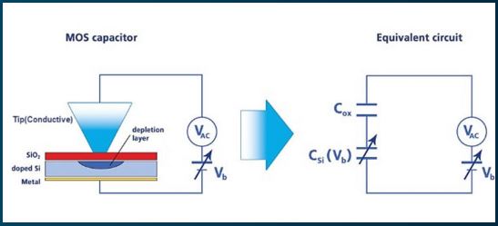
Figure 1. MOS capacitor formed by the conductive material coated SCM tip and the semiconductor sample, which both act as electrodes with an AC voltage applied between them. In the equivalent electrical circuit, the semiconductor oxide layer and the depletion layer act as capacitors in series.
Generally, SCM measures spatial capacitance variations on semiconductors and thereby maps the carrier concentration and doping profiles in non-uniformly doped samples. The application of SCM for failure analysis in the semiconductor industry continues to grow since SCM maps localized charges and electronic defects with a nanometer resolution. For example, SCM is applied to characterize the gate oxide in metal-oxide-semiconductor (MOS) devices: As the gate oxide gets thinner due to the reduction of overall device dimensions, problems and failures can occur, caused by charges trapped in the oxide layer during device operation. Presently, no other characterization tools are able to locally resolve the location of the failure and the electrical defects in two dimensions. In addition, SCM is used in the field of ultrahigh density nonvolatile semiconductor memories. Here, stored charges in the insulator layer of the metalinsulator-oxide-semiconductor (MIOS) heterostructure of the non-volatile memory can be imaged with a nanometer resolution by the SCM.
SCM operates with a conductive materialcoated AFM tip and a highly sensitive capacitance sensor in addition to regular AFM components. By applying an AC voltage, the conductive tip in contact and the oxidized semiconductor sample form a MOS capacitor with the tip and sample acting as electrodes. This MOS capacitor consists of two capacitors in series: one is the insulating oxide layer and the other is the active depletion layer near the oxide/silicon interface as shown in figure 1. The total capacitance is determined by the oxide thickness and the thickness of the depletion layer, which depends on the carrier concentration in the silicon substrate and the applied DC voltage (Vb ) between the tip and the semiconductor. Figure 2 (next page) shows DC bias dependence of the capacitance as high frequency C-V curves for p-type (in red) and n-type (in blue) semiconductor samples. Samples with different dopant types display opposite slope directions in their C-V curves. Figure 2 (b) shows DC bias dependence of the differential capacitance derived as derivative from the C-V curve in figure 2 (a).
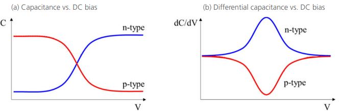
Figure 2. DC bias dependence of the capacitance (a) and the differential capacitance (b) for n-type and p-type doped semiconductors in blue and red, respectively.
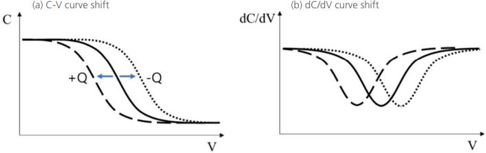
Figure 3. Positive or negative trapped charges in the insulating layer on a p-type doped semiconductor cause a parallel shift of the capacitance drop to lower and higher voltage values, respectively, in the high-frequency C-V (a) and dC/dV curve (b).
The presence of trapped charges in the insulating layer of a p-type semiconductor causes a parallel shift of the capacitance drop in the high-frequency C-V curve along the voltage axis. Depending on the nature of the trapped charges, this shift is either to higher (negative charges) or lower voltage values (positive charges) in the C-V and the dC/dV curves as shown in figure 3 (a) and (b), respectively.
Figure 4 (next page) describes the detection scheme of dC/dV measurements for a p-type semiconductor sample with heterogeneous doping concentration. The AC voltage applied by a lock-in amplifier generates capacitance variations in the sample’s depletion region at fixed DC bias. The lock-in amplifier then detects variations in the amplitude and phase of the sample’s capacitance signal at the same frequency as the applied AC voltage. However, no absolute capacitance values are measured. In other words, the lock-in amplifier output is equivalent to the differential capacitance (dC/dV). Therefore, SCM detects the differential capacitance at fixed DC and AC voltage as the tip moves across the sample and images different regions in carrier concentration in phase and amplitude.
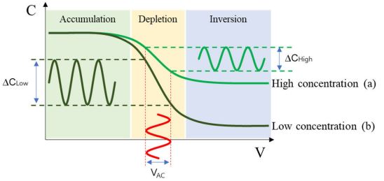
Figure 4. The detection scheme of dC/dV measurements depends on the doping concentration of a semiconductor sample. Shown here is an example of a p-type semiconductor.
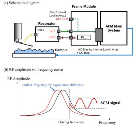
Figure 5. Schematic diagram of SCM operation principle (a). The RF resonance frequency is shifted by the change in the tip-sample capacitance (b).
For different doping concentrations as shown in figure 4 (a) and (b), the slope of the C-V curve in the depletion region changes. The capacitance drop of a highly doped sample is less distinct than for a sample with a low doping concentration. Here, the SCM amplitude detected by the lock-in amplifier is measured with reversed contrast with doping concentration of the sample. When the doping concentration is low, then the SCM amplitude shows higher contrast because the low concentration makes higher depletion layer when the same VAC is applied like figure 4. Figure 5 (a) shows the experimental setup of capacitance measurement via SCM. It consists of a resonator circuit with three lines: The first line depicts a radio frequency source (RF), that is connected to the frame module and contains a phase-lock loop (PLL) to generate an RF signal and a power amplifier to amplify it. The second line is an RF adopting line connected to the RF detector. The third line is the capacitance sensor line along the tip. A capacitance oscillation between the tip and the sample changes the resonance characteristic of the resonator via the RF detector line, which results in a difference of the output voltage amplitude from the RF adopting line. As shown in figure 5 (b), this RF changes due to the capacitance difference of the sample while scanning.
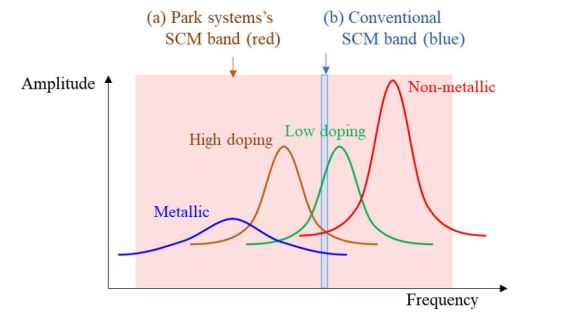
Figure 6. Comparison of a operating frequency band in Park Systems’ SCM mode (red) and conventional SCM (blue). Resonance curves of different materials are plotted as a reference. Park Systems AFMs cover a much wider SCM frequency range and thereby sensitively characterize a multitude of different materials.
In figure 6, SCM resonance curves on different samples are shown. The shape and the position of the resonance curve vary with different materials or doping concentrations. For example, the resonance frequency of metals is relatively low, while the resonance of dielectrics is relatively high. Conventional SCM uses RF oscillators with a fixed and limited operating frequency range as shown in figure 6 (b), which lowers the image qualities and SCM sensitivity on metallic and dielectric samples. Park Systems’ SCM on the other hand operates over a wide frequency range with a tunable frequency to select the optimal resonance frequency and quality factor to optimize each measurement. The SCM probe is connected to a RF-resonator, which has an internal variable capacitor that allows adjusting the probe to select an optimum resonance frequency and quality factor. Since the sensitivity is proportional to 1/√BW, a higher frequency provides higher sensitivity. The SCM probe with variable operating frequency covers a wide RF band from 600 MHz to 2,000 MHz. This allows for maximized resolution and sensitivity by enabling the user to always choose the operation frequency at the maximum slope of any SCM resonance curve, as exemplified in figure 5 (b). In addition, the innovative electrical shielding and dielectric probe holder of the SCM probe allow for measurements with reduced stray capacitance and increased signal-to-noise ratio. Not only the SCM probe holder but also the SCM sensor is important. As the SCM sensor operates within the RF range, the electro-magnetic radiation from the resonator to the metallic structures in the vicinity causes stray capacitance. Therefore, unnecessary radiation should be minimized through proper insulating and shielding. For this reason, we avoided metallic materials for the mechanical parts in the vicinity of the probe by using a ceramic material instead.
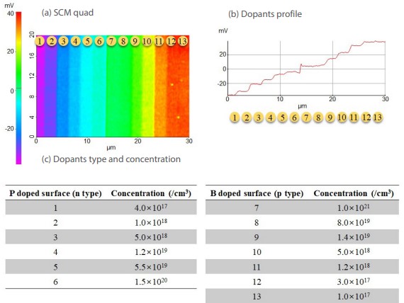
Figure 7. P doped (n-type) and B doped (p-type) surface with different doping concentration. SCM quad image (a) which is combined signal of SCM amplitude and SCM phase (SCM Quad = Amplitude × cos (phase)). SCM amplitude represent the doping concentration and SCM phase represent the type of dopants. And dopants profile (b) and the specification of the sample for dopants type and concentration (c).
Also, the length of the wiring from the SCM resonator to the probe was minimized, and the size of the opening at the front of the resonator was optimized. As shown in figure 7, SCM measurements allow distinguishing n and p implanted surfaces having different doping concentration. The sample has n and p implant areas on p Si substrate, covered with a thin oxide layer about 3 nm (figure 7 (a)). Number 1 to 6 is a phosphorus n-type surface and number 7 to 13 is a boron-doped p-type surface. Figure 7 (b) shows the dopants profile with 13 different doping levels and the doping type. The negative part of the SCM line profile represents the n-type and the the postive part of the line profile represents the p-type doped surface. Figure 8 (next page) shows a dopantprofile study to control the parameters of semiconductor processing using SCM. N-poly is planted in a silicon-on-insulator wafer (SOI) as shown in the cross-section view of the sample structure in figure 8 (a). The topography and SCM quad image were taken at the top of the sample surface before (figure 8 (b)) and after annealing (figure 8 (c)). The SCM images as well as the dopant line profiles (figure 8 (d)) were changed after annealing process. The SCM line profile demonstrates a well defined dopant-type an shape of n-poly.
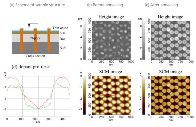
Figure 8. Schematic sample structure of n-poly implant silicon on insulator (SOI) wafer surface (a), AFM height and SCM images before annealing (b) and after annealing (c), and the dopants profile comparison (d) of before annealing (red) and after annealing (green).


