


With the continuous decrease in device sizes and critical dimensions in the semiconductor industry, the ability to measure electrical properties locally with a high spatial resolution is vital for accurate device characterization and failure analysis. Here, Atomic force microscopy (AFM) offers real space imaging of local surface properties on the nanoscale. Conductive AFM (C-AFM) in particular, simultaneously measures the topography and conductivity of a sample by scanning the surface with a conductive material coated tip as a nanoscale electrical probe at an applied DC bias. The current distribution at the given bias is detected via a current amplifier and visualizes heterogeneities in the local conductivity. In addition, current-voltage (IV) spectroscopy on a single point, multiple points or an area can also be collected in C-AFM. Generally, C-AFM is a common technique to study electrical properties of a wide range of materials, including nanoparticles, nanowires, carbon nanotubes, 2D materials, thin-film coatings, and bulk materials. It is applied for leakage current evaluations, failure analysis of semiconductor devices, and on/off switching properties of diodes. Combined with the high voltage toolkit, pinpoint nano-mechanical mode, and/or a temperature control stage with customized sample holders, C-AFM on Park AFMs can be customized as required and operates under various measurement conditions.
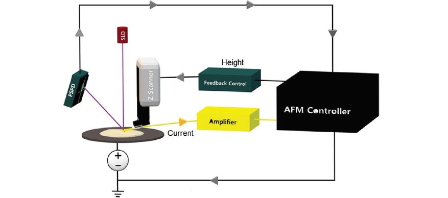
Figure 1. Schematic of the C-AFM set-up, where a conductive material coated tip is connected to a current amplifier (in yellow), which detects the current signal at a given DC bias, applied via the sample holder. The height feedback simultaneously regulates the Z scanner for a constant tip-sample force.
In principle, the operation of the C-AFM is similar to Scanning tunneling microscopy (STM): a bias voltage is applied between tip and sample and the current or tunneling current between the two is measured. However, the main differences between the two modes are the type of probe and the feedback signal used for scanning. STM uses a sharpened metallic wire/tip and maintains a constant tip-sample distance with a feedback based on the tunneling current between the metallic wire and conductive sample. C-AFM scans the surface with a conductive cantilever, with a metal- or doped diamond coated or full-metal tip, while the feedback maintains a constant cantilever deflection and thereby a constant tip-sample force. Since C-AFM operates in contact mode this tip-sample force lies in the short-range repulsive interaction regime. Moreover, STM is limited to well-conducting samples so that a sufficiently high tunneling current is detected at the applied bias, while C-AFM has no limitation for the sample materials such as conducting materials, semiconductors, and composite of conducting/non-conducting materials.
During C-AFM imaging, a conductive tip scans the sample surface in Contact mode while simultaneously measuring the current flow at each pixel for a given sample bias with a current-to-voltage preamplifier as shown in figure 1. Since the magnitude of the electric current can range from a few pico-amperes to milli-amperes depending on the sample, the current amplifier should be chosen to match the conductivity of the respective sample. Park Systems offers three different options for the current amplifier to fit the requirements of a wide application range. The first option uses an internal amplifier, the second option includes an external variable gain, low noise current amplifier (VECA), and the third option is an external ultra-low noise current amplifier (ULCA). The measurable current ranges and specifications of each amplifier are given in Table 1.
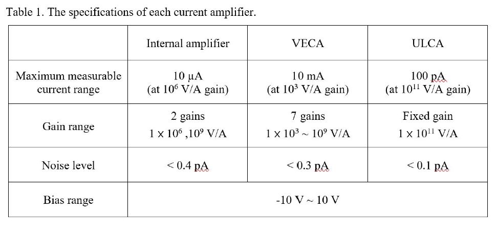
The internal current amplifier of Park AFMs measures currents up to 10 μA. A total of six gains are available with the internal amplifier depending on the current signal range of the sample: two pre-gains for low noise and four post-gains for high-speed imaging. The VECA, with its variable gain setting, is adaptable to a wide range of conductivities and detects currents up to 10 mA. For electric currents in the pico-ampere regime, the electrical noise has to be suppressed to femto-ampere. Here, the ULCA, with its ultra-low noise circuit design, can measure currents in the range of 0.1 pA to 100 pA, as required for accurate characterization of samples with low conductivity. Furthermore, Park AFMs can apply DC biases from -10 V to 10 V. However, by connecting the high voltage amplifier a bias range of -150 V to 150 V is available.
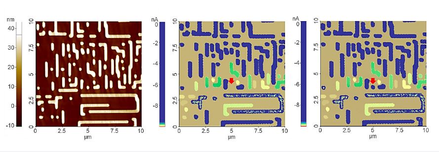
Figure 2. C-AFM measurement on semiconductor devices with integrated circuits for failure analysis. (a) Sample height, (b) current image of a good device, and (c) current image of a bad device. The red arrows in (b) and (c) highlight the position of a failed device component.
Figure 2 shows a C-AFM measurement on semiconductor devices for failure analysis using the internal current amplifier. The devices were scanned with a 10 μm by 10 μm scan size and -0.5V sample bias. The height image (a) visualizes the positions of device components that are protruding from the surface. Both current images in (b) and (c) show different conductivity levels of the device components with respect to the substrate. However, the current image on the failed device (c) clearly illustrates a high leakage current on one of the components that is absent in the current image of the good device (c). This leakage current can result in device failure due to a short-circuit.
Besides imaging the current distribution at a given DC bias, C-AFM facilitates current-voltage (IV) spectroscopy. IV spectroscopy measures the current as a function of the DC bias that is swept forward and backward within a predefined bias range at a given rate. Thereby, IV spectroscopy locally resolves IV characteristics, which are required, for example, to investigate the operating properties of semiconductive devices. Park Systems' IV spectroscopy mode allows either a free selection of multiple points within an image, or mapping IV curves over a volume area using a grid function as shown in figure 3 on an SRAM device. The sample height (a) and the current distribution (b) were measured via C-AFM scanning with a 10 μm by 10 μm scan size and a sample bias of -0.5 V. The height image features protrusions on the surface, which exhibit different conductivities in the current image. Subsequent IV spectroscopy mapping from -1 V to +1 V was performed with 32 by 64 points in a 2 μm by 5 μm area at the position marked red in (a) and (b). From each IV curve within the grid, the current distribution at a certain bias can be reconstructed for -1 V, 0 V, and 1 V in (c) – (e), respectively. Analysis of the IV data shows that the protrusions respond differently to the applied bias: While some of the protrusions are only conductive at negative bias, others are only conductive at a positive bias. Two single IV curves in (f) measured at points 1 and 2 in (c) and (e) illustrate the different IV-behavior.
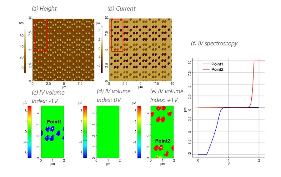
Figure 3. C-AFM and IV spectroscopy measurement on an SRAM device. The sample height (a) and current (b) with the area of the IV map shown in red. IV volume images at -1 V (c), 0 V (d), and +1 V (e) samples bias show different conductivities at a given bias. IV spectroscopy curves at point 1 and 2 in (c) and (e) are shown in (f).
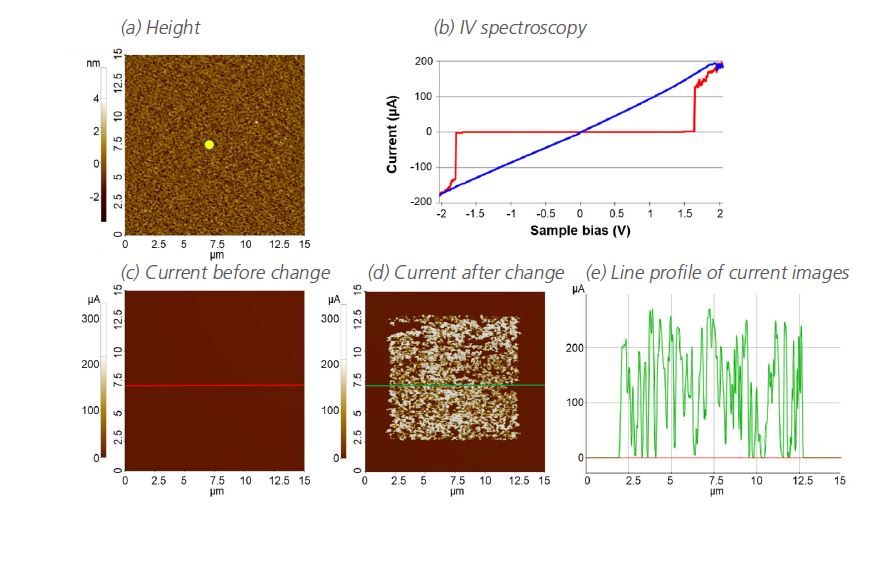
Figure 4. C-AFM experiment in an NiO sample using the VECA for current detection. (a) Sample height, (b) IV sweep from -2 V to +2 V (red) and reverse (blue) showing the sharp increase of the current above the threshold voltage (IV position marked yellow in (a)). Current images at 1 V sample bias before (c) and after (d) changing the conductivity in a 10 by 10 μm area by applying 2.5 V sample bias. The line profiles extracted at the position of the red and green lines in (c) and (d) to visualize the sudden increase in current (e).
Figure 4 summarizes a C-AFM experiment using the VECA to image the current distribution on a NiO surface. Prior to the scan, an IV spectroscopy measurement (b) was performed to check the sample current range in dependence on the applied sample bias. In the forward sweep, the sample bias gradually increased from -2 V to +2 V (red) and in the backward sweep the bias decreased from +2V to -2V (blue). The sample showed no current signal for sample biases between -1.8 V and +1.7V in the forward sweep. However, once the sample bias exceeded ±1.7V, the threshold voltage, the detected current suddenly increased and the sample maintained the high conductivity in the backward sweep. Thus, the IV spectroscopy data suggests that the sample conductivity is permanently changed once the threshold voltage is exceeded.
Current images in figure 4 (c) and (d) confirm the conductivity change above the threshold voltage. No current signal was detected with +1 V sample bias during the initial scan in (c) with a scan area of 15 μm by 15 μm. To change the electrical conductivity a subsequent 10 μm by 10 μm measurement applied +2.5 V sample bias, which is above the threshold voltage. Image (d) shows the current signal of the third C-AFM measurement with +1 V sample bias, after the change of the surface conductivity during the second scan. The differences in current measured before and after applying 2.5 V at the same position are clearly visible in the current images and line profile in (e). Since the current range of the sample after changing its conductivity is on the order of hundreds of μA, the 104 V/A current amplifier gain was chosen to cover the sample’s current range on the VECA, therefore achieving a maximum measurable current of up to 1 mA.
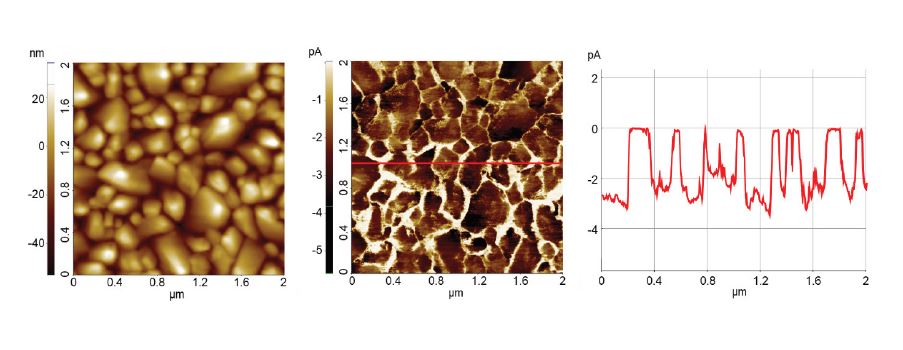
Figure 5. C-AFM measurement of pentacene on Ni by the ULCA at -4 V sample bias. (a) Sample height, (b) current image and (c) line profile extracted at the red line in (b).
Figure 5 demonstrates the ability of Park Systems' C-AFM to measure small currents on the order of just a few pA on a pentacene coated Ni sample. The sample was scanned with 2 μm by 2 μm scan size, a sample bias of -4 V and the current signal was measured using the ULCA, which has 1011V/A current gain. The maximum measured current value on the sample was as low as -3 pA on top of the bulk grains, while the current signal of the grain boundaries was zero. The line profile in (c) furthermore shows the remarkably low noise level that the ULCA can achieve.


