


Ahram Kim (Research Product Management of Park Systems, Seoul, Korea)
Piezoelectric material has been widely used as the actuator of the positioning scanner in an atomic force microscope (AFM) since the invention of the AFM1. It has been used not only in the academic instrumentation, but in the commercial AFM products because of its simplicity in structure, and its possibility to move continuously in the nanometer scale. However, it has also been associated with hysteresis and creep errors that prevented conventional AFMs from providing an accurate topography of a sample. Park has developed Park NX10 featuring a very low noise Z sensor that enables a true topography AFM scanning of a sample.
In the early stage of the AFM development, the open-loop scanning method was used to control the scanner. Here, the scanner moves as the piezoelectric actuator expands and contracts in response to the calibrated applied voltage. This was soon replaced by the closed-loop scanning method2 because the open-loop method introduced nonlinear errors of hysteresis and creep errors to the AFM image. The closed-loop scanning method employed additional position detectors to each axis of the scanner, and applied voltage to the scanner to correct and keep its position at the desired location. Subsequently, the closed-loop scanning method became indispensible for the accurate scanner control. However, the closed loop feedback was limited to the X and Y directions of a sample surface and not on Z (height) direction due to the significant noise level on its Z position detector.
When applied voltage to Z scanner was used as topography, hysteresis of piezoelectric actuators caused errors. The position error was pronounced as edge overshot at the leading and trailing edges as shown in Figure 1(a). In addition, the voltage required regular calibrations as the piezoelectric actuator aged. Piezo creep was caused by the intrinsic materials property of a piezoelectric actuator that drove the Z scanner. The only way to correct this artifact was to use an independent position sensor that directly measured the topography.
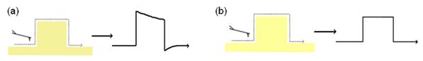
Figure 1. (a) The topography obtained from the voltage signal applied to the Z scanner. The nonlinear nature of the piezoelectric scanner such as creep and hysteresis introduced errors to the real topography. (b) The topography from the low noise Z position detector. Note, the noise level of the Z position detector has to be insignificant to be used as the true sample topography.
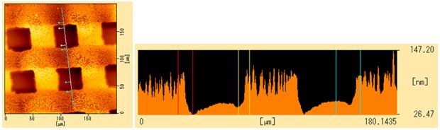
Figure 2. (a) A typical example of an AFM image with edge over-shoot phenomena. (b) The line profile shows Z scanner overshoots when it meets steep height changes.
Now, recent AFM development of Park NX10 features a very low-noise Z position detector with 0.02nm noise level (shown in Figure 3), a noise level low enough to replace the applied voltage to the Z scanner as the topography signal. The topography images in Figure 4, acquired by Park XE-100 and Park NX10, show the surface of the same sapphire wafer. Both of the topography images obtained from the Z voltage signal, Figure 4(a) and 4(c), show the atomic steps of the material, while the image from the Z position detector of the NX10, Figure 4(d), shows the atomic steps with identical quality. The image obtained from Park XE-100, Figure 4(b), picked noise from the Z position detector.
The advantage of the topography acquired by the low-noise Z position detector is evident when a sample has a well-defined steep height change as shown in Figure 5. The 1-µm step-height Z calibration sample (TGZ04, Mikromasch) was measured using Park NX10. The acquired image by the applied voltage, Figure 5(a), shows the overshoot, making a flat top area look slanted. The overshoot appears only at abrupt height changes, something that is very difficult to correct using software even with a higher order correction. The image acquired from the Z position detector, Figure 5(b), on the other hand has no such artifact, rendering a true topography of the sample.
As the demand in research for accurate result has heightened, technological advances have followed to meet this requirement. The closed-loop scan method, and the decoupled XY-Z scanner structure3 are contributing to this need by increasing the scanner’s positioning accuracy. The low-noise Z position detector of Park NX10 now adds new accuracy to the AFM technology with true sample topography of the sample surface.
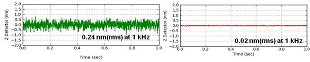
Figure 3. The noise level of the Z position detectors of (a) the Park XE-100 and of the (b) Park NX10, respectively.
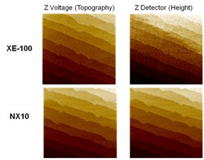
Figure 4. The topography images of a sapphire wafer obtained from XE-100 and NX10
Figure 4. The topography images of a sapphire wafer obtained from (a) the applied voltage to the Z scanner and (b) the Z position detector of Park XE-100, respectively. The noise level of the Z position detector of Park XE-100 is not sufficient to distinguish the atomic steps of the sapphire wafer. However, the topography images of the same sapphire wafer obtained from (c) the applied voltage to the Z scanner and (d) the Z position detector of Park NX10, show the atomic steps. The height information from the Z position detector shows identical noise level with the Z voltage signal. The scan size of the all the images is 3 µm × 3 µm.
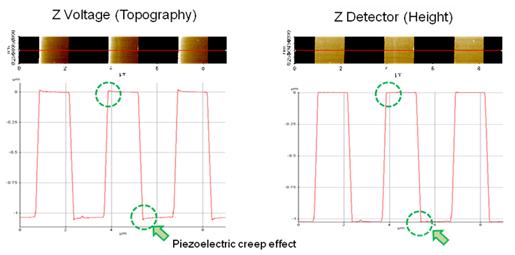
Figure 5. (a) The topography of the 1-µm step-height grating obtained from the driving bias signal to the Z scanner. (b) The topography from the Z position detector.
Reference
1. G. Binnig, C. F. Quate, and Ch. Gerber, Phys. Rev. Lett. 56, 930 (1986).
2. R. C. Barrett and C. F. Quate, Rev. Sci. Instrum. 62, 1393 (1991).
3. J. Kwon, J. Hong, Y-S Kim, D-Y Lee, K. Lee, S. Lee, and S. Park, Rev. Sci. Instrum. 74, 4378 (2003).


