


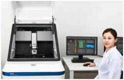
Park Systems, a leading manufacturer of Atomic Force Microscopy systems since 1997 announced PinPoint Counductive AFM, an extremely accurate conductive measurement technology at nano-scale resolution for failure analysis (FA) in the semiconductor industry.
 PinPoint Conductive AFM is designed to integrate
with Park Systems NX20 Atomic Force Microscope
and other Park AFM Products. PinPoint Conductive technology
has succeeded in solving all of the shortcomings
of conventional conductivity AFM such as quick tip wear,
degradation of resolution, low signal to noise ratio,
no tip pressure control, and poor reproducibility of data
Santa Clara, CA September 25, 2013
Park Systems, a leading manufacturer of Atomic Force Microscopy systems since 1997 announced PinPoint Conductive AFM, an extremely accurate conductive measurement technology at nano-scale resolutionfor failure analysis (FA) in the semiconductor industry. The PinPoint Conductive technology provides on-location electrical conductivity data at specific points on sample to researchers and failure analysis engineers. What that means is that scientists and engineers can now acquire contact current measurement at any specific location of a sample at varying tip pressures, and at a much higher accuracy and precision than what has been possible to-date. Added benefits from this technology are frictionless conductivity scanning, reproducible data from repeated measurements, cost savings from longer lasting AFM probe tips, and sustained super high nano-resolution. The PinPoint Conductive AFM is designed to integrate with popular Park NX20 and Park NX10, the leading choice for atomic force microscopy in the research and semiconductor industry.
“Conductive AFM is an important tool for device research and failure analysis, and PinPoint Conductive technologyhas succeeded in solving all of the shortcomings of conventional conductivity AFM such as quick tip wear, degradation of resolution, low signal to noise ratio, no tip pressure control, and poor reproducibility of data. The conventional conductive AFM prevalent in the industry has to sacrifice the spatial resolution as the tip wears out in contact mode or the current level due to short and limited contact time,” explains Ryan Yoo, Vice President of Global Sales and Marketing. “The newly developedPinPoint Conductive AFM provides the best of both higher spatial resolution and optimized current measurement.”
In PinPoint Conductive mode, the AFM probe monitors its feedback signal, approaches towardsthe sample surface until a predefined threshold point, measures the Z scanner’s height, then it rapidly retracts. The XY scanner stops during the electric current acquisition, and the contact time is controlled to assure enoughtime for quality data acquisition. PinPoint Conductive AFM allows higher spatial resolution with optimized current measurement over different sample surface; furthermore, it does not apply any lateral force thanks to the decoupled vertical movement of the Z scanner of the cantilever.
PinPoint Conductive was designed to replace the conventional contact conductive AFMand is an enhanced design that eliminates the problems of the tip wearing out during contact mode topography and diminished contact time. Park’s PinPoint Conductive AFM enables engineers and research scientists to characterize and confirm electrical designs of semiconductor device structures with much more accuracy, precision and confidence in the data.
About Park Systems
Park Systems serves its customers by providing a complete range of atomic force microscopy (AFM) solutions, backed by its global service and support. Park Systems is the leading nanotechnology solutions provider for nanoscale measurements and systems for both research and industry. The product line of Park Systems reflects its focused strength to help customers achieve the metrology performance that meets the needs and requirements of present and future applications. Since improvements in nano-metrology are key to enabling tomorrow's research, analysis, processing and product manufacturing, the innovative technology and market leadership of Park Systems in the field of nano-metrology will remain as the core competence and market driving force of its future business. Park Systems has its global manufacturing and R&D headquarters in Korea. Park’s products are sold and supported worldwide with regional headquarters in the US, Korea, Japan, and Singapore, and distribution partners throughout Europe, Asia, and America. For more information, visit http://www.parkAFM.com .


