


Gerald Pascual, Byong Kim, and Keibock Lee
Technical Marketing, Park Systems Inc., Santa Clara, CA
The goal of all forms of microscopy is to enable the observation of increasingly smaller objects and their details and characteristics which cannot be seen without aid. Naturally, the course of scientific investigation demands that we eventually test the absolute limits of available metrology techniques and Atomic Force Microscopy (AFM) is no exception. AFM has been demonstrated to be capable of generating images with resolutions high enough to visualize sample features measured in fractions of nanometers—such images are often referred to as having achieved a so-called "atomic resolution." However despite this moniker, the resolution of these images is not at a level detailed enough to reveal individual atoms, but rather only the resonance of the spaces between atoms that make up materials with atomically flat surfaces [1, 2, 3], such as graphite or mica. The surfaces of these materials are arranged in uniform lattices with constants that are only several tenths of a nanometer wide and are being scanned with probes which feature tip radius curvatures that are greater in size by an order of magnitude (2-5 nm). A fresh tip detecting the resonance of features smaller than its radius curvature can be compared to an open palm running over the keys on a keyboard. By using tactile feedback one can render a mental image of the approximate layout of the keyboard, but would have great difficulty in making out single keys. Modern AFM systems, including those produced by Park Systems, are capable of producing "atomic resolution" images with features as small as few tenths of an angstrom, but the distinction of imaging by resonance versus imaging solely from the cantilever feedback response must be made. Until probe manufacturing has advanced to a point where tip radius curvatures can be on the order of widths of single atoms, innovations in ultra-high resolution AFM must come from other avenues.
Since the true resolution limit of AFM imaging is dependent on the geometry of the probe tip, logic dictates that to maintain the highest image quality for the longest amount of time consideration must be taken to preserve tips during and across multiple scans. Contact mode, the most basic AFM operation technique, requires the probe to be dragged across the surface of the sample in order to obtain topography data. The nature of this tip-sample engagement makes probe blunting a concern as higher tip radius curvatures result in decreased spatial resolution and therefore less accurate imaging. Increased long-term supply expenses to maintain stocks of contact mode probes are an additional concern for many laboratories. To maintain the highest ultra-high resolution for the longest duration and in the most cost-effective manner, AFM images should be taken in non-contact mode instead. In this operation technique, an oscillating probe's tip's distance from the sample surface during a scan is maintained by a precise, high-speed feedback loop. These state-of-the art electronics, such as those found in NX-series system architecture from Park Systems [4] keep the probe in the non-contact regime of the van der Waals forces between the atoms of its tip and those of the sample. Deviations in the amplitude of the probe's oscillation are recorded as the probe traces over the sample and are then used to create topography images. As the tip and probe do not make direct contact during scanning, tip longevity is dramatically increased with no observable loss in resolution over dozens of scans [5].
Demonstrating the efficacy of non-contact mode for ultra-high resolution AFM imaging requires a challenging sample with features that rival the smallest tip radius curvatures of commercially available AFM probes. To further strengthen the argument for non-contact mode's increased tip longevity across multiple scans, the sample must also be regarded by the research community for its difficulty as a subject for consistent, reproducible nanoscale imaging. Nanomaterials that meet both of these criteria are those that feature moiré patterns. These are secondary and visually evident patterns that are a result of periodic patterns (such as atomic lattices) being placed on top of one another and are then rotated to create a new distinct and offset design. Repeatable high resolution imaging of moiré patterns and the super lattice constants which comprise them present significant challenges if not done with non-contact mode AFM because the resolution that has to be achieved is about the size of the tip radius curvature. Any loss in tip sharpness such as the blunting effect prevalent in AFM modes other than non-contact, would introduce an unacceptable handicap to the repeatability of data acquisition. Combating this obstacle to produce any kind of serviceable AFM image and data, let alone one at an ultra-high resolution for the technique, is a tall order even for experienced AFM operators as hardware limitations and constant scan parameter optimization through trial-and-error further complicate the task. Removing any kind of additional disadvantage that increased tip deterioration would pose is a welcome reprieve for this application.
The ultra-high resolution of AFM, together with the advantages of modern system architecture and robust automation software, was demonstrated in a graphene/hexagonal boron nitride (hBN) sample evaluation conducted by Park Systems using a Park NX10 AFM system powered by Park SmartScan operation software. The sample consisted of an hBN substrate overlaid with a graphene layer and was scanned under ambient air. The purpose of the evaluation was to assess the Park NX10's ability to characterize the topography of the moiré pattern that was created when one layer was set on top of the other and offset by rotation. Using non-contact AFM mode and a standard AFM probe tip [6], the Park NX10 was able to successfully image the moiré pattern super lattice constant of the sample [7] in scans as large as 500 x 500 nm (see Figure 1a). A second scan (see Figure 1b), this time at 250 x 250 nm, was collected referencing a single isolated sample defect in the upper-left quadrant of the initial 500 x 500 nm scan as a landmark. The super lattice pattern around the defect in the center is now even more visually evident than before.
The Atomic Force Microscopy has provided those in research and industry with high resolution nanoscale measurements and imaging, but has long been limited by its relatively slow imaging speed. For certain applications such as crystal nucleation and growth, materials transportation and protein self-assembly process [1-3], it is important to keep track of the topography changes and particle transportation. For such studies, an AFM needs to be able to image as fast as possible without overly sacrificing the data accuracy and repeatability required to reproduce the work. In order to meet this challenge, engineers from Park Systems have pushed themselves to improve their existing AFM systems to scan at an increased frequency without loss of resolution and accuracy and the need for any additional costly setup.
Today, with Park's NX series of AFM systems and high frequency cantilevers, one can generate AFM images at the expected high resolution while maintaining a significantly increased scan speed compared to legacy systems. All Park NX series AFMs are built for fast Z scanner feedback speed and optimized Z servo control so only an ultra-high frequency cantilever is all that is needed to carry out high-speed AFM imaging. Park's Fast Imaging is the most optimized solution to the need for expedited AFM image generation. This enables the researcher to perform fast and accurate imaging of sample surfaces covering a wide spectrum of feature heights, ranging from single nanometers to tens of nanometers.
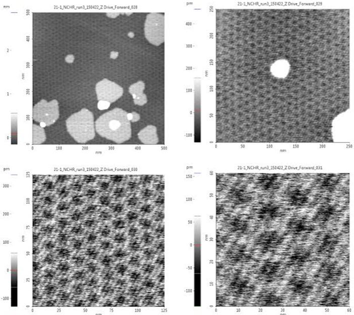 Figure 1. A series of four non-contact AFM topographical images of a graphene sample exhibiting moiré patterns: (a) at 500 x 500 nm, (b) at 250 x 250 nm, (c) at 125 x 125 nm, and (d) at 60 x 60 nm. All images were taken with a Park NX10 AFM system using the Park SmartScan operating software's Auto mode.
The final two scans in the series serve as the most compelling evidence in demonstrating the Park NX10's ability to maintain its ultra-high resolution even after multiple scans with the same AFM tip. In Figure 1c, the diagonal striations superimposed onto the moiré pattern become evident as they repeat across the surface of the sample. The final image in the series, Figure 1d, was taken at a scan size of 60 x 60 nm and provides the clearest evidence that not only are the super lattice constants of the moiré pattern about 15 nm [7] in width, but that the spacing between each striation on the moiré pattern is roughly 4-5 nm in length. Observations of such striations in graphene/hBN systems have been previously reported [8]. This latter distance is in line with the expected tip radius curvature values for the AFM tip used to acquire all four sets of data. Given the consistency and clarity of the data as the acquired images increase in magnification and the generally accepted difficulty of the sample to characterize with AFM, this achievement is truly remarkable. This accomplishment of resolving five nanometer periodic features is compounded even further when one considers that this data can now be collected by inexperienced researchers guided by the automation software. These demonstrated advantages of non-contact mode for ultra-high resolution AFM imaging can only become more valuable as tip radius curvatures decrease and the effect of tip blunting becomes more pronounced as we characterize smaller and smaller features on our samples.
Acknowledgements
We are thankful to Patrick Gallagher of Stanford University for providing the graphene/hBN sample used to acquire the images presented in this report.
REFERENCES
[1] Park, S. Ultimate Resolution of AFM in Air. Retrieved from https://drive.google.com/open?id=0BxAebzniH1MvWjQyWkFXUTlHanM (2004).
[2] Mizes, H., Park, S., & Harrison, W. Phys. Rev. B 36 4491 (1987).
[3] Albrecht, T.A., Mizes, H.A., Nogami, J., et al. App. Phys. Lett. 52, 362 (1988)
[4] Park NX10 – Technical Info. Retrieved from http://www.parkafm.com/index.php/products/research-afm/park-nx10/technical-info (2016)
[5] True Non-Contact™ Mode. Retrieved from http://www.parkafm.com/index.php/park-spm-modes/91-standard-imaging-mode/217-true-non-contact-mode (2016)
[6] AFM tips PPP-NCHR. Retrieved from http://www.nanosensors.com/PointProbe-Plus-Non-Contact-Tapping-Mode-High-Resonance-Frequency-Reflex-Coating-afm-tip-PPP-NCHR (2016)
[7] Zandiatashbar, A. Automated Non-Destructive Imaging and Characterization of Graphene/hBN Moiré Pattern with Non-Contact Mode AFM. NanoScientific, Fall 2015 14-17 (2015)
[8] Gallagher, P., Lee, M., Amet, F., et.al. Nature Comm. 7 10745 (2016)


