


High Throughput and Non-Destructive Sidewall Roughness Measurement Using 3-Dimensional Atomic Force Microscopy
Yueming Hua, Cynthia Buenviaje-Coggins (Park Systems Inc., CA, USA)
Yong-ha Lee, Sang-il Park (Park Systems Corp., Suwon, Korea)
ABSTRACT
As the feature size of the semiconductor device is becoming increasingly smaller and the transistor has become three-dimensional (e.g. Fin-FET structure), a simple Line Edge Roughness (LER) is no longer sufficient for characterizing these devices. Sidewall Roughness (SWR) is now the more proper metric for these metrology applications. However, current metrology technologies, such as SEM and OCD, provide limited information on the sidewall of such small structures. The subject of this study is the sidewall roughness measurement with a three-dimensional Atomic Force Microscopy (AFM) using tilted Z scanner. This 3D AFM is based on a decoupled XY and Z scanning configuration, in which the Z scanner can be intentionally tilted to the side. A sharp conical tip is typically used for imaging, which provides high resolution capability on both the flat surfaces (top and bottom) and the steep sidewalls.
Keywords: AFM, critical dimension, LER, sidewall roughness, FinFET, EUV, Photoresist
1. INTRODUCTION
The AFM has been widely used in universities for research purposes, and it has also been used in the industry as a metrology tool. One of the main applications of the AFM in metrology is height measurement. There are many different AFM height measurements; it could be a simple step height measurement, CMP dishing measurement, pole tip recession (PTR) measurement for hard disk read/write head [1], trench depth measurement, or some other type of measurement. The AFM is also used for surface roughness measurement. However, because most AFMs operate in a top-down configuration, the AFM has a limited access to the sidewall. This is especially true when the sidewall angle is close to, or greater than 90 degrees. To overcome this obstacle, certain AFM technology is able to use the side of a flared tip to image the sidewall [2]. However, the flared tip is quite blunt compared to the sharp conical tip, and it weakens the resolution on the sidewall. In addition, a flared tip is much more difficult to make, and its quality is hard to control. A temporary solution has been used to characterize the sidewall roughness by mechanically cleaving the sample and then imaging the sidewall with AFM on tilted sample with regular conical tip. But this method only works for large features and it is destructive to the tip itself, as its sharpness fades in the process.
Recently, Park Systems has introduced a new Park 3D AFM imaging technology using tilted Z scanner with a sharp conical tip for imaging [3]. When the tip tilts, it can easily reach the sidewall of the sample features,even when the sidewall angle is close to, or over 90 degrees. This new technology is extremely powerful for sidewall roughness measurement. In this paper, we have also studied the throughput and repeatability of this new Park 3D AFM technology as a metrology solution for sidewall roughness.
2. Park 3D AFM WITH TILTED Z SCANNER
The new Park 3D AFM is based on a decoupled XY and Z scanning system [4]. In this decoupled scanning configuration, the XY scanner is a 2D flexure scanner. It moves the sample only in the XY direction and is independent from the Z scanner. The Z scanner is driven by a high force multi stack piezo element that moves the tip only in the Z direction (Figure 1-A). The independent Z scanner allows the tip to be intentionally tilted to easily access the sidewall (Figure 1-B). The tilted scanner design allows CD measurement at the top, middle, and bottom of the lines, as well as roughness measurement along the line’s sidewall. The method builds upon the standard AFM tip design resulting in a technique that a) maintains the same resolution as the traditional AFM, b) that can be used with sharpened conical tips for best image resolution, and c) that does not suffer from corner inaccessibility from limited shape of tips with large radius.
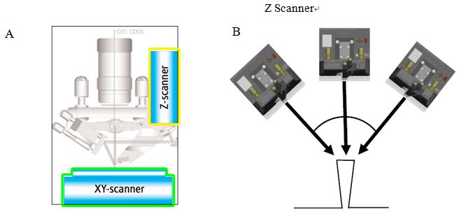
Figure 1, A. decoupled XY and Z scanning system; B, 3D AFM using tilting Z scanner
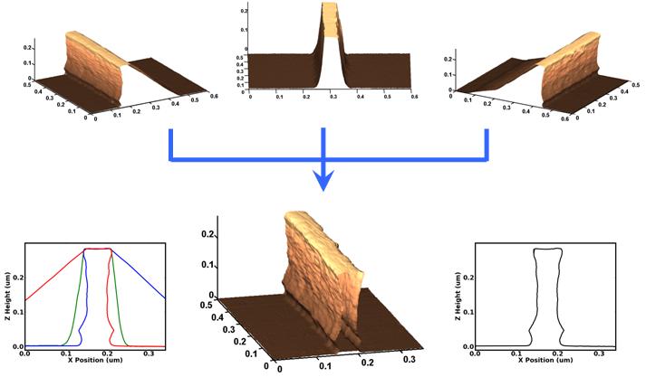
Figure 2.Imaging with Park 3D AFM
In order to take a full 3D image, the AFM typically scans at three tilted positions (center, left and right) to acquire three images. Each of these three images provides different information. For example, the image acquired at left tilted position provides detailed information on the left sidewall, as well as the top and bottom surface. These three images can be combined together to form a full 3D image of the feature (see Figure 2). The full 3D image provides detailed 3D information of the feature that is imaged, such as the top CD, middle CD, bottom CD, LER, LWR, sidewall angle, etc. [5]. Because a sharp conical tip is used, the tip can access the very small structures at the bottom of the feature, such as the small undercut at the very bottom of the photoresist line as seen in Figure 2.
3. SIDEWALL ROUGHNESS MEASUREMENT
As Park 3D AFM uses the same feedback mechanism as regular AFM, it can also use the regular sharp conical tip for AFM imaging. One main factor which determines the imaging resolution is the sharpness of the tip. Compared with other types of tips (e.g. cylindrical tip or flared tip), the conical tip is best in sharpness that enables Park 3D AFM to provide the best resolution for the sidewall imaging. For sidewall imaging, the Z scanner can be fixed at one tilted position, and scan along the sidewall for significantly higher throughput.
Figure 3 shows a Park 3D AFM image of a photoresist line. This image was taken by scanning in the direction along the line. The scan resolution is 256 pixels in X direction and 512 pixels in Y direction. This image shows high resolution information on both flat surfaces (top and bottom) and the sidewall. On the sidewall, the very rough and detailed grainy surface of the photoresist is visible, but the top and bottom surfaces are much smoother.
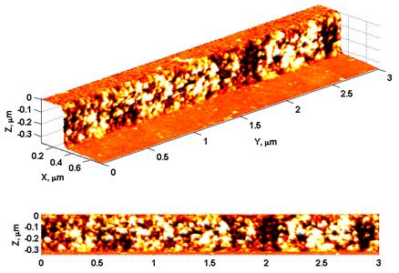
Figure 3. 3D AFM image of the sidewall of a photoresist line
Single line profiles on the top, sidewall, and bottom surface can be extracted from the high resolution 3D AFM image. Figure 4 shows the single line profiles at different surface of the photoresist. These line profiles also clearly show that the sidewall is much rougher than the top and bottom surfaces.
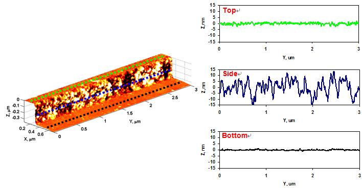
Figure 4. Profiles of a photoresist line at different surfaces
This Park 3D AFM sidewall image of the photoresist provides more detailed information about the sidewall surface than the traditional metrics (e.g. LER). This information is very useful in photoresist research and photolithography process development.
Park 3D AFM with sharp conical tip not only provides high resolution image of the sidewall, it also measures the sidewall roughness with very high precision. Repeatability was tested with five sites and ten repeats. Table 1 shows the testing results. The average sidewall RMS roughness of the tested photoresist sidewall is about 6.1 nm. The Standard Deviation (STD) of the sidewall roughness measurement is about 0.20 nm or better for each individual site. And for the 5-site wafer average sidewall roughness, the measurement STD is 0.08 nm, which is only about 1.3% of the measured roughness.
Table 1. 5-site 10-repeat data of sidewall roughness measurement
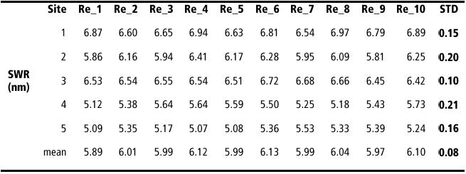
Figure 5 plots the 5-site average roughness of all the ten repeats. The plot shows that the roughness has stayed very consistent over the ten repeats, and there has been no pattern that shows it is increasing or decreasing during the repeated measurements. This means that the tip has remained as sharp as it was before the 50 measurements were done. Meanwhile, the soft photoresist was damaged only after ten repeated measurements. This is expected during the measurement because the AFM is operated in non-contact mode.
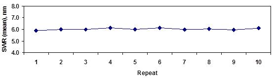
Figure 5.5-site average roughness of 10 repeats
During the repeatability test, each image was scanned for 32 lines along the sidewall direction, and each line has 512 data points. The image scan range is 0.5 um across the photoresist line, and 3um along the photoresist line. Each measurement took about two minutes. Of these two minutes, the image scanning took about one minute for each image (32 lines at 0.5 Hz). The sample navigation and alignment took another one minute, which included the stage moving, optical pattern recognition, AFM alignment, and tip approaching.
This throughput could be further improved. When we scanned 32 lines over 0.5um across the photoresist line, about half of the line was on the top or bottom surface. Sixteen lines over 0.3um should have been sufficient to cover the sidewall surface with a decrease in the line density on the sidewall. By reducing the scan range along the photoresist line from 3.0um to 1.5um, the tip could scan at 1.0 Hz without compromising the surface tracking at the same settings. Hence, the scanning time for each image could be reduced to 16 seconds. With further optimization of the materials and procedure, the sample navigation and alignment time could be further reduced to about 45 seconds, resulting the throughput to about 1minute/site.
4. CONCLUSIONS
Park 3D AFM using tilted Z scanner with sharp conical tip provides high resolution sidewall imaging. It is also non-destructive and provides high throughput. Park 3D AFM can precisely measure the sidewall roughness with measurement STD of 0.08nm (5 site average) for the sidewall roughness of about 6.1 nm. Park 3D AFM can be used in applications, such as Fin-FET Device Characterization, EUV Photoresist Evaluation, Etching Process Fine Tuning, Photolithography Process Development, OPC Optimization, and OCD Calibration, among others.
ACKNOWLEDGEMENTS
Thanks to Dr. Jane Frommer and Ms. Linda Sundberg at IBM Almaden Research Center for providing some interesting samples.
REFERENCES
[1] Joonhyung Kwon, Yong-Seog Kim, Kwanseok Yoon,Sang-Min Lee, Sang-il Park, "Advanced nanoscale metrology of pole-tip recession with AFM", Ultramicroscopy 105, 51–56 (2005)
[2] Bharat Bhushan, Harald Fuchs, and Masahiko Tomitori, Applied Scanning Probe Methods VIII, Springer, 31-75 (2008)
[3] Sang-Joon Cho, Jung-Min Lee, Byung-Woon Ahn, Joonhui Kim, Young Yoo, Yueming Hua, Sang-il Park, “Three-dimensional imaging of undercut and sidewall structures by atomic force microscopy”, Review of Scientific Instruments, 82, 023707 (2011)
[4] Joonhyung Kwon, Jaewan Hong, Yong-Seok Kim, Dong-Youn Lee, Kyumin Lee, Sang-min Lee, Sang-il Park, “Atomic force microscope with improved scan accuracy, scan speed,and optical vision”, Review of Scientific Instruments 74, 4378-4383 (2003)
[5] Yueming Hua, Cynthia Coggins, Yong-ha Lee, Jung-min Lee, Kyung-deuk Ryang, Sang-il Park. “New 3-Dimensional AFM for CD Measurement and Sidewall Characterization”, Proceedings of SPIE (2011), Vol. 7971, 797118