


John Paul Pineda, Cathy Lee, Christina Newcomb, Gerald Pascual, Byong Kim, and Keibock Lee
Park Systems Inc., Santa Clara, CA, USA
ABSTRACT
Magnetization reversal plays a major role in designing the switching mechanisms of magnetic nanostructures in a high density storage device. In this study, magnetization reversal in a magnetic patterned array sample was successfully investigated using an atomic force microscopy (AFM) system via magnetic force microscopy (MFM). The magnetic property and topography data of a sample surface were obtained simultaneously and the data shows that the two signals are well separated by the two-pass scanning method. The MFM images demonstrate that a majority of the circular dot domain structures with 148 nm width on the sample surface experienced a magnetization reversal during the scan with a few domains remaining in their original state. Some of the circular dots that experienced a magnetization reversal switched their magnetization easily, while others switched gradually as the magnetic field between the tip and the sample changes over time. A single defect was also observed in the images of the acquired data. The results sum up that the technique described in this study can provide a reliable data in understanding the magnetization behavior and can be used in defect identification of a magnetic sample.
INTRODUCTION
Magnetic storage is vital to the digital era, and is implemented in a wide variety of devices including computers, cell phones, data servers, and others. The ability of magnetic storage devices to inexpensively store large amounts of information in a small area makes it attractive compared with other high-density storage technologies [1]. Maintaining a high signal to noise ratio (SNR) has become a great challenge in high density recording. One of the most effective methods for achieving an adequate SNR involves storing the data in a magnetic patterned array. In this method, the data are stored in lithographically defined magnetic patterns in the form of magnetic domains with each domain representing a single data bit which can be either a 1 or a 0 bit. The magnetic properties of the nanostructures such as domain magnetization, shape, size, array spacing, etc. can greatly affect the performance of the magnetic storage device. Thus, a technique that can measure these characteristics and investigate samples with nanoscale features must be utilized in evaluating device reliability. There are several methods that can be used in investigating and monitoring magnetic domains. Examples include Photo Electron Emission Microscopy (PEEM), Scanning Electron Microscopy (SEM), X-ray Magnetic Circular Dichroism (XMCD), Kerr Effect Microscopy, among others [2, 3, 4, 5]. However, some of these methods do not provide high spatial resolution; while others have tedious sample preparation requirements, are destructive, or do not operate in ambient conditions. For these reasons, Magnetic Force Microscopy (MFM) was developed to overcome such shortcomings. In addition, the integration of the two techniques enables the user to acquire both topography and magnetic property data simultaneously without changing the sample or tip. To this end, MFM was used to investigate a magnetic patterned array and the data shows that this technique is an effective method for the magnetic properties characterization of magnetic storage devices.
EXPERIMENTAL
A magnetic patterned array sample was investigated using a Park NX10 Atomic Force Microscopy (AFM) system. The magnetic properties of the sample were characterized under ambient air conditions using MFM mode. A cantilever with a tip coated with a magnetic material (Nanosensors, PPP-MFMR) was magnetized prior to imaging and used in the entire experiment. A non-magnetic sample holder was also utilized to obtain an optimum measurement. The MFM measurements were performed using the conventional non-contact two-pass scanning method (see Figure 1). Four consecutive images were acquired at the same position at 4 minute intervals to observe the magnetic domain variation over time.
In MFM mode, there are two interaction forces between the magnetized tip and the magnetic sample: the Van der Waals force and magnetic force. The van der Waals force is harnessed to generate the sample's surface topography while the magnetic force between the magnetized tip and magnetic sample generates data for the sample's magnetic properties. The obtained cantilever oscillation signal contains both sets of information; therefore, a method that can completely separate these signals is the key to successful imaging. One such method introduced to accomplish this task is two-pass scanning. In this method, the topography data is obtained in the first scan while the MFM data is obtained in the second scan. The tip is lifted during the second scan in the height where the only change in force affecting the cantilever oscillation signal is the change of the magnetic force as shown in Figure 1 [6]. In this experiment, the optimum value of tip-sample distance chosen to get a reliable MFM image is 50 nm. A lock-in amplifier which is embedded in the AFM system is used to analyze the tip motion caused by the van der Waals force in the first scan and magnetic force in the second scan. In MFM mode, the domain structures and polarity are detected by analyzing the changes in the cantilever's oscillation frequency caused by the magnetic field. The magnitude of the change in oscillation frequency is proportional to the magnetic field intensity. During scanning, the tip is either attracted toward or repulsed from the sample surface depending on the domain magnetization of the sample.
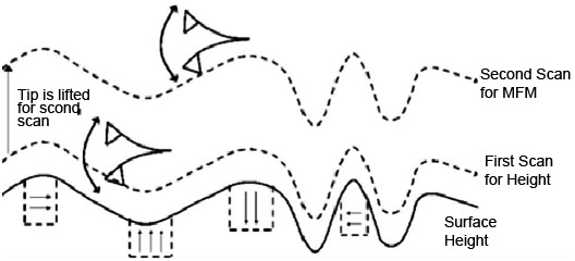
Figure 1. Two-pass scanning method of MFM mode
RESULTS & DISCUSSION
The topography data obtained in this experiment shows that a lattice structure with circular dots was successfully fabricated but no significant information related to its magnetic domain is provided. In contrast, the magnetic property data acquired in MFM measurements shows the magnetic domain structure and magnetization, but no significant information related to physical structure of the sample. The domain structure observed in MFM data of this sample is similar to the physical structure observed in topography data, which is a patterned array consisting of circular dots. The data acquired in this experiment were all analyzed using XEI software developed by Park Systems. Figure 2 shows the topography and MFM measurement of the magnetic patterned array sample acquired at the first time point. The topography data shows a clear image of a well-defined lattice structure. The line profile that was generated by the XEI software in Figure 2 provides the geometrical information of the lattice structure. The data shows that the diameter of each circular region is approximately 148 nm in diameter (Figure 2, red arrows) and 44 nm in height (Figure 2, blue arrows). The array spacing for the circular regions is approximately 71 nm (Figure 2, green arrows). The MFM image shows that the domain structures are also circular and all are bright in color. The contrast of the circular dots correlates to the domain magnetization. In this experiment, the bright color implies that the magnetic dipole points in an upward direction normal to the sample surface while a dark color implies a magnetization pointing in the downward direction. Thus, the MFM image demonstrates that the lattice structure at the initial time point is compose of a circular pattern in a magnetic single-domain state that are pointing in an upward direction.
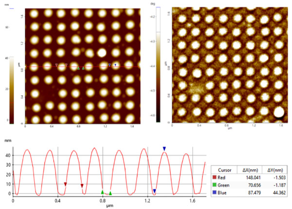 Figure 2. Topography (top-left) and MFM (top-right) data from the magnetic sample. Line profile of AFM topography (Red: circular dot diameter, Green: array spacing, Blue: circular dot height.
Figure 3 shows the MFM measurements acquired every 4 minutes. Based on the color of the circular regions, Figure 3a shows the majority of the circular regions have completely switched magnetization polarization, while some have either partially switched or had no change. The partially switched domains represent a magnetic multi-domain state while the domain that experienced a complete magnetization reversal and those that remained on their original magnetization represents a magnetic single-domain state [7]. From this interpretation, the lattice after 4 minutes is comprised predominantly of single-domain states with a few multi-domain states. By monitoring the individual domains over time, it is observed that most of the single-domain states experienced a complete magnetization reversal. The same interpretation can be made in Figure 3b, however, most of the partially switched domains at the second time point have completely switched their magnetization by the third time point. At the final time point, Figure 3c shows the structure is composed of circular dots that are all in a single-domain state. The majority of these single-domain states are the ones that experienced a complete magnetization reversal pointing in a downward direction. The remaining circular dots with bright colors are the ones that remained at their initial magnetization during the entire process. The absence of the switch in magnetization of these domains could be due to surface non-uniformity [8]. It is speculated that the magnetization reversal is caused by the changed in the magnetic field between the tip and the sample over time.
A surface irregularity on the lattice structure was also observed on the lower left sides of all the images. This irregularity is speculated to be a single defect that was acquired during the fabrication process [9, 10]. Such individual defects could greatly affect the magnetic reversal properties of the sample [10].
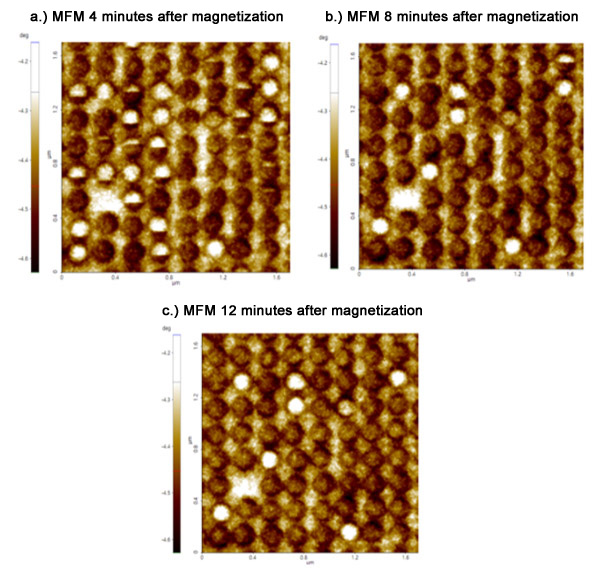
Figure 3. a.) MFM data 4 minutes b.) 8 minutes and c.) 12 minutes following magnetization. Scan size: 1.7 um x 1.7 um
SUMMARY
The lattice structure of the magnetic patterned array was successfully characterized by the Park NX10 AFM using MFM mode imaging. The topography data revealed that the lattice structure is composed of circular regions with a diameter of 148 nm and height of 44 nm. The MFM data shows that a majority of the magnetic domains experienced a magnetization reversal during the scan with a few domains remaining in their original state as the magnetic field between the tip and the sample changes over time. A surface irregularity was also observed on the images speculated to be a single defect consisting of a region that does not exhibit magnetic properties likely created during the fabrication process. Characterization of magnetization reversal is significant in designing the switching mechanisms of magnetic nanostructures. A well designed switching mechanism is important especially in writing the information in a bit cell. Failure of inversion of a single bit during writing will lead to data loss or corruption. Overall, the technique described in this study could be used in the investigation of magnetization reversal behavior and defect identification of high-density magnetic storage devices.
REFERENCES
[1] Z. Bandic, et al., Advances in Magnetic Data Storage Technologies. Scanning the issue
[2] K. Koike, et al., Scanning Electron Microscope Observation of Magnetic Domains Using Spin-Polarized Secondary Electrons. Japanese Journal of Applied Physics, Volume 23, Part 2, Num. 3.
[3] P. Kasiraj, et al., Magnetic domain imaging with a scanning Kerr effect microscope. IEEE Transactions on Magnetics, Volume: 22, Issue: 5, Sep 1986.
[4] C. Schneider, et al., Investigating surface magnetism by means of photoexcitation electron emission microscopy. Reports on Progress in Physics, Volume 65, Number 12.
[5] P. Fischer, et al., Imaging of magnetic domains with the X-ray microscope at BESSY using X-ray magnetic circular dichroism. Zeitschrift für Physik B Condensed Matter, December 1997, Volume 101, Issue 3, pp 313–316.
[6] Park MFM Technique: http://www.parkafm.com/images/spmmodes/magnetic/Magnetic-Force-Microscopy-(MFM).pdf.
[7] P. Krone, et al., Investigation of the magnetization reversal of a magnetic dot array of Co/Pt multilayers. Journal of Nanoparticle Research, November 2011, Volume 13, Issue 11, pp 5587–5593
[8] A. Fraerman, et al., Observation of MFM tip induced remagnetization effects in elliptical ferromagnetic nanoparticles. Institute for Physics of Microstructures RAS, Nizhny Novgorod, Russia
[9] A. Manzin, et al., Influence of lattice defects on the ferromagnetic resonance behaviour of 2D magnonic crystals. Scientific Reports 6, Article number: 22004
[10] X. Hu, et al., The influence of individual lattice defects on the domain structure in magnetic antidot lattices.