


NanoInnovation, a conference and exhibition taking place in Rome, Italy from 11 to 14 of June 2019, gives a platform for the multidisciplinary community involved in the development of nanotechnologies and in their integration with other enabling technologies (KETs) in all application fields.
Park Systems and its Italian partner, Gambetti Kenologia are proud to be a part of this event for the third time with a booth and satellite event on site!
- Event Dates: 11-14 June, 2019.
- Venue: Renaissance Cloister by Sangallo at the Faculty of Civil and Industrial Engineering of “Sapienza” University of Rome in Via Eudossiana 18
- Our location: Gambetti Kenologia's Booth
SATELLITE EVENT: Advances in surface electrical characterization at the nanoscale by using Scanning Kelvin probe microscopy (SKPM)
(Seminar and Life Demo):
Date: Wednesday, 12 June, 9am & 14pm
Program (same morning and afternoon):
- Welcome and Introduction
- “Advances in surface electrical characterization at the nanoscale by using Scanning Kelvin probe microscopy (SKPM)“
- Instrument Demonstration on Park NX10 AFM
- Discussion und Summary
ABSTRACT:
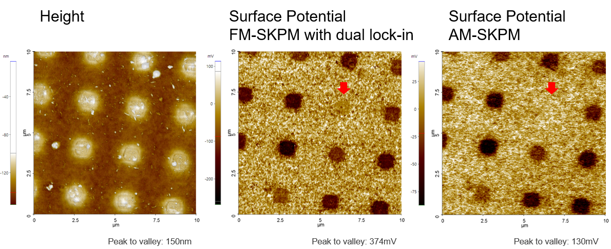
Scanning Kelvin Probe microscopy (SKPM) allows measuring work function and electrical potential distribution of various materials, to provide a better understanding of nanostructures and CMOS semiconductor devices to improve their performance.[1-2] SKPM has also been used to determine quantitative information such as the charge distribution in polymer materials.[3, 4] Compared to other techniques, SKPM is nondestructive and compatible to ambient conditions. Conventional Amplitude Modulation (AM) SKPM has already allowed remarkable enhancements in the field of device reliability, but it is limited by its signal-to-noise detection ability. For this scope Park Systems recently developed Frequency Modulation FM-SKPM. The results show that FM-SKPM is significantly more sensitive than AM-SKPM in measuring surface potential distribution. In this workshop we will demonstrate that FM-SKPM has better sensitivity in detecting surface potential variation of polymer material in comparison to AM-SKPM. In fact, FM-SKPM provided higher resolution with sharper edges of the domains and detected smaller potential variations than AM-SKPM on the same irregular surface.
REFERENCES
1. Lan Fei (2018) Fundamentals of Kelvin Probe Force Microscopy and its applications in the characterization of solar cells. Doctoral Dissertation, University of Pittsburgh.
2. J. Pineda, et al., Electrical Characterization of Semiconductor Device Using SCM and KPFM Imaging. https://www.parksystems.com/index.php/applications/electrical-electronics/semiconductor/612-electrical-characterization-of-semiconductor-device-using-scm-and-kpfm-imaging
3. J. Gonzalez, et al., Charge distribution from SKPM images, PCCP, Issue 40, 2017.
4. M. Ortuño, et al., Conducting polymers as electron glasses: surface charge domains and slow relaxation, Scientific Reports volume 6, Article number: 21647 (2016). tion.
SPEAKER:
Dr. Andrea Cerreta – Application Scientist at Park Systems.
Image capture:
10x10 µm2 image of a polymer-patterned array. Topography image (left), FM-SKPM image (center), and AM-SKPM image (right).
Join the seminar and live demo to learn more about advantages of FM-SKPM!
Link: More information HERE