


Dr. Alain Diebold,
SUNY Polytechnic Institute
AN INTERVIEW WITH DR. ALAIN DIEBOLD INTERIM DEAN AT THE COLLEGE OF NANOSCALE SCIENCE AT SUNY POLYTECHNIC INSTITUTE AND NATHANIEL CADY, PHD, ASSOCIATE PROFESSOR OF NANOBIOSCIENCE SUNY POLYTECHNIC INSTITUTE
Dr. Alain Diebold is Interim Dean at the College of Nanoscale Science at SUNY Polytechnic Institute, Empire Innovation Professor of Nanoscale Sciences, and Executive Director, Center for Nanoscale Metrology. Dr. Diebold earned his BS in chemistry from Indiana University- Purdue University, and holds the PhD in Statistical Mechanics of Gas-Solid Surface Scattering earned at Purdue University. He is Associate Editor of the IEEE Transactions on Semiconductor Manufacturing as well as the Metrology Section of Future FAB International. A frequent presenter at international conferences, Dr. Diebold has been named a Fellow of both the International Society for Optics and Photonics (SPIE) and the American Vacuum Society (AVS).
Since 2005, Dr. Diebold has presented at over 45 leading conferences on Frontier Metrology and Characterization for Nanoelectronics. He is recognized industry-wide as a leader in cutting edge research on advanced metrology methods to improve nanoelectronics.
Dr. Diebold has published close to a hundred research papers and made over 40 presentations world-side. He has established a long career in nanometrology and nanoscale semiconductors and has done continuous work for decades with industry to collaborate on the development of new methods and technology.
His books include Handbook of Silicon Semiconductor Metrology. He is co-editor of Frontiers of Metrology and Characterization for Nanoelectronics, Characterization and Metrology for ULSI Technology, Semiconductor Characterization: Present Status and Future Needs, Analytical and Diagnostic Techniques for Semiconductor Materials, Devices, and Processes.
“WE ARE DEVELOPING A NEW FORMAT OF NEUROMORPHIC HARDWARE, LEVERAGING UNIQUE PIECES OF HARDWARE TO BUILD A HYBRID SYSTEM,” SAID DR. CADY. “THEY ARE LIKE ELECTRONIC DEVICES THAT MIMIC SYNAPSES IN THE BRAIN.” THE GOAL OF THE RESEARCH IS TO HAVE A BETTER ABILITY TO DO THINGS AUTONOMOUSLY SUCH AS AUTONOMOUS CARS FOR INSTANCE AND DEVELOP SPECIALIZED HARDWARE THAT REDUCES POWER USAGE COMPARED TO THE TRADITIONAL SOFTWARE APPROACH.
Neuro Morphic Computing –
How Materials and Devices with “brain like” Architecture are Revolutionizing Computing
Nanometrology Advances and Challenges
When asked what the latest in new designs for more complex device structures and advanced new materials is, Dr. Diebold explains that Nanowire type transistors fabricated from multi-layer thins are emerging as the news technology. In the past, finfet was made from silicon. Silicon nanogratings with fin-like nanogroove arrays have been used in nanoelectronics to build field effect transistors (FinFETs), which have attracted enormous attention due to their superior electronic properties. They can also be used in photonic systems to achieve desired linear and nonlinear optical functionalities.
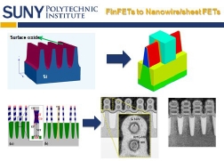
But more recently multi-layer Silicon Nanowire and Silicon Nanosheets with gates all around the transistors and a lot of 3D structure at being researched. “It is very difficult to do the metrology,” explains Dr. Diebold. “And it is hard to predict when or if this will be commercialized.” There are metrology challenges with Nanowires is the Dielectric gate, spaces, and wires. There are advances in all of the typical nanometrology tools especially TEM. One of the key factors in today’s nanometrology research is automated TEM analysis dual column; it is becoming more prevalent as a critical new advancement due to much higher throughput characterization. One of the most significant future trends in the semiconductor industry as Dr. Diebold looks into the future are automated TEM analysis that feed into hybrid metrology. “The goal of Hybrid Metrology is to use the measurement information from multiple methods to improve 3D determination of feature shape and dimensions,” explains Dr. Alain Diebold. AFM enables the determination of surface and sidewall roughness and feature line shape and is often used in conjunction with TEM, CD-SEM, and Scatterometry in Hybrid Metrology.
The von Neumann architecture is replaced with neuro morphic architecture
The semiconductor industry is definitely going in a new direction explains Dr. Diebold. He does not see the future of silicon chips
continuing to scale the way they have for the last twenty years. “Silicon chips for the future are going to be more functional, computing like the brain,” he explains. “Neuro Morphic computing is a new way of computing with different architecture to act neuromorphic.”
At SUNY, research on neuro morphic computing is well underway. In Jan of 2016, Dr. Nathaniel Cady at Associate Professor of Nanobioscience at SUNY Polytechnic Institute was awarded $1.2 million from the Air force Research Lab as part of a $2.4 million grant in collaboration with the University of Tennessee, Knoxville enabling the fabrication and testing of a dynamic, adaptive neural network based on memristors, cutting edge technology which could one day lead to faster, more energy efficient and powerful computer capabilities.
The extra computing power of neuromorphic computing comes at a time when industry has hit a limit and won’t be able to continue to make the leaps in speed and density they did over the past decades. “Neuro computing augments the chip by building unique hardware that adds functionality,” explains Cady.
The neuromorphic computing market is poised to grow rapidly over the next decade to reach approximately $1.78 billion by 2025. For the Air Force grant, they are creating unique, non standard materials for neuro synapses. Professor Cady said that he does not characterize what they are doing as AI (artificial intelligence). “The end game is to create a whole brain, by starting with a small set of neurons,” said Cady.


