


 Dr. Christoph Friedrich Deneke,
LNNano, Brazilian Nanotechnology National Laboratory
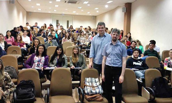 Dr. Christoph Friedrich Deneke shown above with students studying at LNNano
An interview with Dr. Christoph Friedrich Deneke
What area of scientific discipline do you focus on and what type of research are you doing?
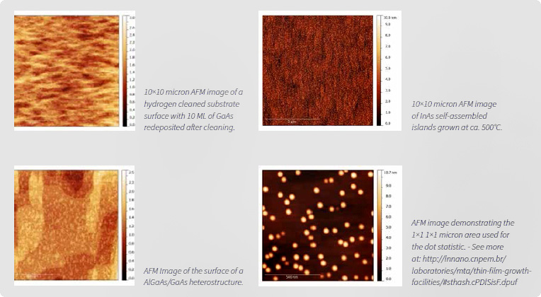
Our group inside the Brazilian Nanotechnology National Laboratory (LNNano) runs the scanning probe microscopy facilities. We are an open user facility doing also in-house research. Therefore, our area of science and interested is quite board and ranges from condensed matter physics with a focus on semiconductor epitaxy to general material science and surface characterization of samples from our users. In more detail, we are studying the formation of self-assembled nanostructures in the InGaAs system on complained membranes, but are also involved in general scanning probe microscopy techniques applied from magnetic characterizationof steel to electrical characterization of diverse systems like graphene oxide or polymers derived from celluloses.
Can you describe your research and what the benefits are?
Our in-house research is focused on molecular beam epitaxy (MBE). As pointed out some years ago in a Nature Nanotechnology article, MBE is one of the funding techniques of nanotechnology. It allows the perfect crystal growth of different semiconductor materials on each other, so called heterostructures. Such structures are used in our days to provide high quality electrical, optical and electro-optical devices such as lasers and heterojunction bipolar transistors.
We investigate the growth of semiconductor heterostructures in the III-V system. In classical epitaxy, bulk semiconductor wafers are used for material deposition – we want to use compliant, extremely thin semiconductor membranes as substrates. Our investigation started with basic growth studies to understand, how the material behaves on these novel substrates and aims for the creation of well know device structures in the III-V system.
We hope that with these compliant substrates allow a new class of semiconductor device. We think that we can grow heterostructures that cannot be grown on classical bulk wafer substrates.
Why is your work important in today’s society?
The trend in modern computer and semiconductor technology request stronger integration. Furthermore, we have to reduce the energy footprint for environment, but also for customer application – everyone complains, the smartphone drains the battery too fast, right? We hope to address these demands with our research making computers less energy hungry, help to improve integration and the production less resource demanding. Our work as an open user facility benefits directly the Brazilian society by educating a new generation of Brazilian researchers and helping the research community to gather their results.
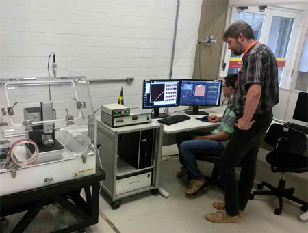 Dr. Christoph Friedrich Deneke, LNNano, Brazilian Nanotechnology National Laboratory, pictured with Park NX 10 at the LNNano Surface Science Lab
How do you use Atomic Force Microscopes in your work?
For our in-house research, we use AFM mainly for topographic images of the samples after material deposition. It is our standard tool to judge the sample quality, characterize the diffusion behavior of the deposited material and understand how to change the parameters of the epitaxial growth. For our users, we offer a large variety of AFM based techniques, with electric force microscopy or Kelvin force microscopy being the important ones. In the last year, we started to rediscover the know technique to do capacitance coupling providing new insides in the samples.
What features of Park AFM do you feel are most vital for success and how is it important in your process?
We like the new Smartscan software, which makes the acquisition of the standard AFM images in high quality very easy. Furthermore, the large flexibility of the Park NX10 (one of our three AFMs) is important for us. The availability of various techniques as well as a third integrated lock-in makes the instrument the microscopy of our choice for EFM measurements as well as the capacitive coupling techniques.
What advancements do you see in the future using AFM that can enhance or improve current methods?
The development of user-friendly interfaces and software is very important. We have a lot of users from – let’s call it – non-classical AFM fields like Dentists, organic chemistry or Archology. Whereas the new Smartscan software provides a very easy interface and therefore easy access to AFM, we miss the same functionality for techniques like MFM or EFM. Currently, we help those researchers with data acquisition and evaluation, but easier software and interfaces will open these methods to a completely new group of users.
What areas of scientific knowledge will benefit from your research?
We contribute mainly to the broad are of classical nanoscience or nanotechnology as well as to semiconductor science. We add to the understanding, how to integrate selfassembled nanostructures into functioning semiconductor devices.
Describe how your research can be applied in industry?
Semiconductor industry is struggling with the integration of III-V material into classical silicon architectures. Whereas we will not solve this problem – simply because of the tremendous complexity of making computer chips and memory devices – we hope, we can contribute and show a possibility, how one could achieve this in the future.
What do you see in future developments in your area of research?
The past has shown that MBE and semiconductor epitaxy are one of the backbones of nanotechnology and information processing. I assume, it will keep its roll there and we will have to educate many generation of semiconductor growers, not only for basic research but also for industry. It seems that in the research environment there is a shift away from basic studies to device oriented research showing how the field becomes more device and application oriented.


