


The sharpness of the tip and the tip-sample distance determine the ultimate resolution.
"What is the ultimate resolution of AFM in air?" This is a very important question because we all want to know the size of the smallest details on our samples an ambient AFM can show. By looking at the 'atomic resolution' images of graphite or mica, such as in Fig. 1, it is natural for us to expect atomic scale resolution from ambient AFM. However, sooner or later, we all realize that AFM cannot show atomic-scale details on our own samples and the following questions arise.
1. If the AFM can demonstrate 'atomic resolution' images of graphite or mica, why are such details not shown on my samples?
In order to address this issue, first it is necessary to correct the misconception of 'atomic resolution images' of graphite or mica. Such layered materials have atomically flat surfaces, which are characterized by having a uniform atomic lattice. The lattice constants of graphite and mica are a few angstroms. On the other hand, the radius of an AFM probe tip is a few nm at best. Furthermore, when the tip makes contact with the sample surface, the tip blunts considerably. (All 'atomic resolution' images of graphite or mica are taken in contact mode AFM.) Therefore, it is unreasonable to expect to image individual atoms with contact mode AFM in air. The 'atomic resolution' AFM images such as in Fig. 1 are not images of individual atoms. They are images reflecting the average spacing of atoms on the sample surface.[1,2] For example, when we pull a large luggage bag over a floor which is uniformly covered with small balls, we can feel a vibration, the period of which is determined by the spacing of the small balls. By collecting the vibration signal, we can form a periodic lattice image of the floor. In this analogy, however, we are not imaging the individual balls, and we would not notice if a ball or two were missing. Likewise, the AFM image of graphite in Fig. 1 shows the 'atomic lattice pattern,' not individual atoms. Therefore, we should use the term 'atomic lattice,' rather than 'atomic resolution.' Such atomic lattice images do not mean much, since they show only the lattice constant, which can be measured by other means.
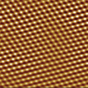 Fig. 1 – AFM image of HOPG taken with XE-100 (5 x 5 nm, modified image from raw data).
This image shows the atomic lattice, not individual atoms.
2. Can ambient AFM have true atomic resolution at all?
Taking atomic resolution images with AFM is a very challenging task even in a controlled environment, such as vacuum or liquid. In ambient conditions, the dynamics of air molecules and the meniscus force of liquid layers on the sample surface prohibit true atomic resolution images with the AFM.
3. Isn't it important to demonstrate atomic lattice images anyway?
One may still argue that atomic lattice images can indicate the stability of an AFM system. Having a better-looking atomic lattice image, however, does not necessarily mean better resolution of the system, since the ultimate resolution of AFM is much larger than the atomic lattice constant of graphite or mica. The difference in system stability between an AFM demonstrating perfect atomic lattice images and another AFM whose atomic lattice image looks a bit noisy is typically less than one angstrom in a lateral direction. While sub-angstrom instability in x-y positioning may make the atomic lattice image look imperfect, it does not make any difference in imaging actual samples where the expected ultimate resolution is a few nm.
Ironically, AFMs that show perfect atomic lattice images would not be desirable. In order to produce better atomic lattice images, the AFM system must have a very compact mechanical structure, which would allow only small scan ranges, tiny sample sizes, and provide restricted sample access. It would be unwise to sacrifice user convenience by limiting the sample size and scan range for the sake of obtaining a better quality atomic lattice image, considering that the ultimate resolution of ambient AFM is not limited by such mechanical structures. The important images are those of the samples in which we are interested, not atomic lattice images.
4. Then what is the ultimate resolution of AFM?
The ultimate resolution we can expect in ambient AFM is similar in scale to the radius of the AFM tip, which is about 2-5nm. Unfortunately, the sharpest part of the tip is very fragile. Once the tip touches the sample surface, no matter how soft the contact or gentle the tapping, the tip becomes blunt instantly. Therefore, it is not possible to achieve the ultimate resolution with contact mode or tapping mode AFM. The ultimate resolution can be achieved only in non-contact mode AFM (NC-AFM). [3]
5. Isn't it true that the resolution of NC-AFM is lower than in tapping mode?
This has been another popular misconception that NC-AFM has lower resolution than tapping mode because the tip cannot come close enough to the sample surface. If the tip did come very close to the sample surface, the tip would touch the sample surface occasionally and any contact with the sample would cause the tip to stick due to the meniscus force. In fact, most sample surfaces in ambient conditions are covered with a liquid layer. The probe tip may become stuck in this layer, in which case the cantilever oscillation will stop. Therefore, when NC-AFM is operated with a very small tip-sample distance, even a slight deviation of tip-sample interaction force from the set point can be fatal, unlike in contact mode. This is why the tip has to be significantly far from the sample surface in conventional NC-AFM, resulting in poor resolution. It is a technically challenging task to implement NC mode with a very small tip-sample distance. (Tapping mode was initially used to avoid the difficulty of precise tip-sample spacing control. [4]) Once correctly engineered, however, NC-AFM provides the ultimate resolution of ambient AFM, far surpassing the capabilities of Tapping mode, as shown in Fig. 2.
For more details, please refer to the article 'Tapping Mode vs. Non-Contact mode AFM'.
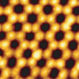 Fig. 2 – AFM image of nano structures patterned on aluminum surface taken with XE-100 (500 x 500 nm).
The fine details on this image demonstrate a resolution of about 2 nm.
[1] H.A. Mizes, Sang-il Park, and W.A. Harrison, Phys. Rev. B 36, 4491 (1987).
[2] T.R. Albrecht, H.A. Mizes, J. Nogami, Sang-il Park, and C.F. Quate, Appl. Phys. Lett. 52, 362 (1988).
[3] Y. Martin, C.C. Williams, H.K. Wickramasinghe, J. Appl. Phys. 61, 4723 (1987).
[4] Q. Zhong, D. Innis, K. Kjoller, V.B. Elings, Surf. Sci. Lett. 290, L688 (1993).