


Nanoscale AFM and KPFM Mapping of Localized Charge and Recombination Centers on Chemically Active ZnO Surfaces
Case Study: Zinc Oxide Surfaces
General Considerations
In recent years, ZnO has gained popularity among researchers due to its excellent ability to grow nanostructures with a variety of unique geometries. Advances in ZnO growth and processing have enabled many opto- and microelectronic applications with nanoscale dimensions such as laser and blue/UV light emitters, yet the impact of surface morphology and near surface defects on optical emission has remained largely unexplored. Techniques such as atomic force microscopy (AFM) and Kelvin probe force microscopy (KPFM) coupled with depth resolved cathodoluminescence spectroscopy (DRCLS) are capable of exploring these features on a nanoscale. Surface morphological features produce near surface defects that affect surface potentials and recombination velocity. This highlights the importance of overall surface quality and surface preparation. Consequently, AFM roughness values coupled with KPFM potential maps may act as a predictive tools for assessing surface optoelectronic quality for nanoscale optical devices. We have used nanoscale DRCLS, AFM, and KPFM to measure the spatial distribution of defects within the outer 10-100nm of the surface of ZnO single crystal wafers grown by melt, hydrothermal, and vapor-phase transport methods.
Park AFM System Overview
At the core of our nanoscale measurements is the Park AFM/KPFM with the Enhanced EFM module. The high lateral and z-axis resolution allows for roughness measurements below unit cell dimensions. This coupled with KPFM potential maps and DRCLS emission allows for accurate determination of optical efficiency. Furthermore, the True Non-Contact mode successfully maintains the tip-sample distance of only a few nanometers allowing for measurements that do not disrupt the surface or its features. This capability is vital for obtaining accurate information about near or subsurface defects and feature that they relate to.
Investigation of ZnO Surfaces
Figure 1 shows DRCLS spectra from two ZnO single crystal sample grown by hydrothermal methods from different sources with relatively high 1(a) and low 1(b) deep level optical emission at that can be de-convolved into contributions from both ~2.1 and 2.5 eV. Previous work has identified the deep level emission at 2.1 and 2.5 eV to be related to zinc vacancies (VZn) and oxygen vacancies (VO), respectively[i]. We may understand the relative densities of these defects by taking the ratio of NBE to maximum defect emission for a given probe energy (EB). For 1(a) (hydrothermal-16) we see that I(NBE)/I(2.1-2.5 eV) at EB = 2 keV results in a ratio R( 2 keV) = 203. The deep level emission changes with excitation energy, first decreasing for EB = 5 keV, then increasing such that R(10 keV) = 84. Figure 1(b) (hydrothermal-1) on the other hand, shows near-surface emission with R(2 keV) = 933. All higher EB spectra show a relative increase in defect emission such that R(5 - 20 keV) ~ 155, i.e. ~6x lower NBE emission efficiency.
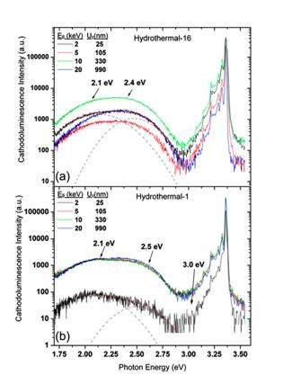
Figure 1. DRCLS spectra of (a) high and (b) low near-surface defect ZnO. The latter shows order-of-magnitude changes in deep level defect emission with depth.[ii]
Figure 2 shows AFM and KPFM maps for both hydrothermal-16 and -1 imaged simultaneously with a Park AFM in Enhanced EFM mode. AFM topography for Hydrothermal-16 (a) reveals rms roughness values of ~2.022 and average roughness values of ~1.505. On the other hand, topography for Hydrotherm-1 2(b) reveals rms roughness value of ~0.644 nm and average roughness values of ~ 0.287 nm. Hydrothermal-16 shows potential changes 2(c) consistent with surface morphology 2(a) due to defects at and below the surface. Circular surface pits (red) with depths ranging from ~2 - 20 nm exhibit potential decreases of greater than 120 mV with increasing radial distance. Conversely, Hydrothermal-1 shows laterally non-uniform potential variations 2(d) due to densities of electrically active defects below the surface. These potential variations of ~ 50 mV do not correlate with any morphological features and are consistent with a smoother surface. This is also consistent with DRCLS spectra that indicate a strong increase in defect densities just below the free surface. The clear reduction of native point defects and surface asperities indicated by both AFM and DRCLS is due to chemomechanical polishing and is a powerful example of the importance of surface preparation.
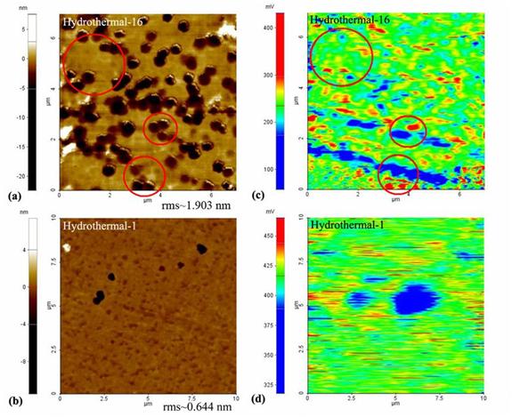
Figure 2. AFM morphology maps (a) and (b) corresponding to hydrothermal-16 and hydrothermal-1, respectively, in Figure 1(a) and 1(b). KPFM potential maps (c) and (d) acquired simultaneously with AFM maps (a) and (b), respectively.ii
We can identify how surface morphology impacts the efficiency of NBE optical emission by introducing native point defects and competing pathways by plotting the ratio of NBE/defect emission as a function of rms and average surface roughness. Figure 3 shows R(2 keV) versus average (a) and rms (b) roughness values for a wide collection of hydrothermal, melt, and vapor phase transport grown ZnO surfaces. We find that rough surfaces exhibit R values ~200 while smoother surface have R > 13,000. Furthermore, both (a) and (b) plots reveal a well-defined threshold dependence. We find that R increases rapidly when surface roughness decreases below a ZnO unit cell of c = 0.52 nm. This suggests that lattice imperfections at the unit cell dimension, rather than extended morphological defects, dominate recombination and NBE intensity.
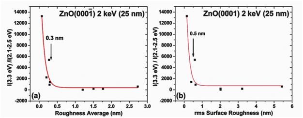
Figure 3. The ratio of NBE to deep level intensities I(3.3 eV)/I(2.1-2.5 eV) for EB = 2 keV for hydrothermal, melt, and vapor phase transport grown ZnO as a function of AFM (a) average roughness and (b) rms roughness displays a well defined threshold dependence that increases rapidly for average roughness <0.3 nm and rms roughness <0.5 nm.ii
The increase in the ratio of NBE to deep level emission and the corresponding relative emission efficiency of NBE radiation is due to lower densities of defects (ND). The sharp increase for roughness’ below 0.5 nm corresponds to a strong ND decrease when roughness is due only to monolayer step edges. Using a modified formalism derived for spherical pores we may estimate the surface charge density within surface asperities as well the overall carrier concentration near the surface[iii].
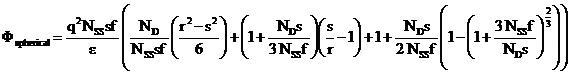
This formalism yields a hemispherical surface pore charge density of 4.2+0.8 x 1011 cm-2 and a carrier concentration of 8.4+0.5 x 1015 cm-3 accounts for the observed 100 meV potential decreases away from the pore perimeter over distances of ~ 125 nm. These potential variations can thus provide a measure of fixed surface charge density within the pore and a bulk free carrier density at the surface.ii
Conclusion
In summary, AFM reveals large variations in surface roughness, asperities, and extended surface features related to growth method and subsequent surface treatments. KPFM surface and subsurface potential variations acquired simultaneously reveal systematic correlations with defect distributions measured by DRCLS. These results stress the importance of surface roughness and surface preparation to minimize surface recombination by free carriers due to defects. The Park AFM scanning probe microscopes non-contact scanning capabilities has proven itself an important tool for understanding material properties and electronic structure without disrupting the surface. The ability to probe the outer few nanometers of any surface and identify the distribution of electrically active defects using KPFM is a powerful tool that can be used to predict surface and optoelectronic quality for nanoscale optical device.
Note
This work was supported by the National Science Foundation under Award No. DMR-0513968 (Verne Hess).
References
[i] Y. Dong, F. Tuomisto, B.G. Svensson, A.Y. Kuznetsov and L.J. Brillson, Phys. Rev. B. 81 (2010) 081201.
[ii] D. Doutt, H. L. Mosbacker, G. Cantwell, J. Zhang, J. J. Song, and L. J. Brillson, Appl. Phys. Lett. 94, 042111 (2009).
[iii] D.C. Look, Z.Q. Fang, S. Soloviev, T.S. Sudarshan, and J.J. Boeckl, Phys. Rev. B. 69 (2004) 195205
By D.R. Doutt and L. J. Brillson