


Why Atomic Force Microscope?
As the design rule becomes smaller, traditional metrology tools, such as stylus and optical profilers, and CD-SEM are unable to meet the precision metrology requirements from magnetic recording industry.
Virtually all the feature sizes in manufacturing steps are in nanoscale, especially that of defect review and pole-tip-recession. Atomic Force Microscope (AFM) routinely performs sub-nanometer measurements in ambient atmosphere, and consequently has gained attention as a new candidate for nanoscale metrology tool. However, old AFM systems based on a piezoelectric tube scanner cannot meet the metrology requirements in the industrial applications due to the intrinsic background curvature and crosstalk between the XY & Z axes.
AFM Products Utilizing Piezoelectric Tube Scanners Cannot Meet the Industry Requirement
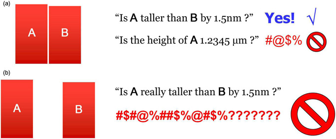
Figure 1.Old piezoelectric tube based AFMs are (a) marginally acceptable in relative dimensioning of two objects right next to each other, but completely useless in absolute dimensioning of an object and (b) even worse in the relative dimensioning of the two separated objects.
The limitation of the piezoelectric tube scanner based AFMs are best demonstrated in Figure 1. Old piezoelectric tube scanner based AFMs are marginally acceptable in relative dimensioning of two objects when placed side by side; however, the problem arises when one needs to know the absolute dimensioning of an object as shown in Figure 1 (a). It gets even worse when two objects are separated as shown in Figure 1 (b); even the relative dimensioning of the two separated objects cannot be performed by the tube based AFMs.
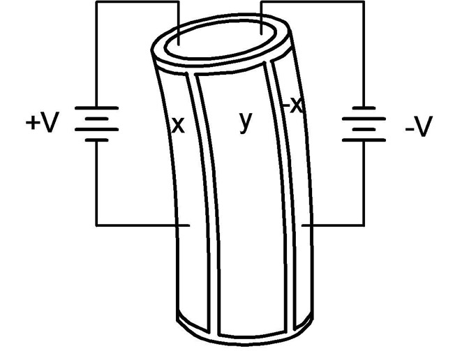
Figure 2. The Piezoelectric tube scanner used in conventional AFMs is not an orthogonal 3-D actuator. Each axis movement is nonlinear, the XY-Z crosstalk with non-linearity inevitably results in a significant background curvature. Moreover, it has a low resonance frequency (< 1 kHz) and low force.
The problem originated from intrinsic limitations with the piezoelectric tube scanner as shown in Figure 2. The piezoelectric tube is made of ferroelectric ceramics that deform by several nm if a voltage is applied to the electrode on the surface. As the piezoelectric tube itself is not orthogonal in three dimensions, and each axis movement is non-linear, the XY-Z crosstalk with non-linearity inevitably results in a significant background curvature as shown in Figure 3. Note that the XY- scanner of old piezoelectric tube based AFMs have more than 80 nm out-of-plane deviation over only 15 μm scan. These conventional AMFs attempt to flatten the background curvature using the second or third order fitting, and due to this every scan data of their AFMs are the result of the “line-by-line” flattening, which is imbedded in their operating software. As a marketing and sales policy, some AFM company engineers are never allowed to demonstrate the raw data of their AFMs (Park Systems can help customers with turning off the imbedded software correction). It is unfortunate that even some of experienced engineers and scientists are deliberately misled to believe that the processed and flattened data of these old piezoelectric tube based AFMs are the raw data.
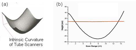
Figure 3. (a) The background curvature of a piezoelectric tube based AFM in raw data and (b) the line-profile cross section of the background curvature. The XY-scanner of old piezoelectric tube based AFMs have more than 80 nm out-of-plane deviation over only 15 μm scan.
The high order fitting and flattening of the background curvatures in piezoelectric tube based ATMs become fatal issues in magnetic recording industry as the feature sizes of manufacturing process become smaller to nanoscale and the absolute AFM dimensioning of such feature is required.
Park Systems AFM Can Meet the Industry Requirements
Introduced by the original innovators and pioneers of AFM technology after 4 years of intensive product development, the Park AFM from Park Systems represents breakthroughs in every aspect of AFM technology (For details, see “The Park AFM: the Technology Behind the True Non-Contact AFM” under XE Mode menu).
Physical separation of the XY-scanner from the Z-scanner completely removes background curvature from the fundamental level, and effectively eliminates the cross-talk and non-linearity problems that are intrinsic to old piezoelectric tube based AFM systems (Figure 4 (a)).3 This uniquely designed AFM systems from Park Systems not only increases the data collecting speed by at least 10 times compared to a conventional piezoelectric tube type scanner, but also improves the error due to the inherent non-linearity of the scanner itself.
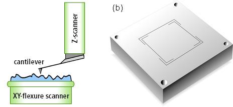
Figure 4. (a) In Park AFM, the Z-scanner is separated from the XY-scanner; the XY-scanner actuates only the sample and the Z-scanner actuates only the probe. (b) 2D guided XY flexure scanner used in Park AFM. This single module parallel-kinematics stage has low inertia and minimal out-of-plane motion, providing the best orthogonality, high responsiveness, and axis-independent performance.
In the Park AFMM, the XY-scanner is a Body Guided Flexure scanner as shown in Figure 4 (b), which is used to scan a sample in the XY direction only. The flexure hinge structure of the XY-scanner guarantees highly orthogonal 2D movement with minimum out of plane motion. Due to the Parallel Kinematics design, the XY-scanner of the Park AFM also has low inertia and axis-independent performance.
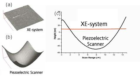
Figure 5. Unprocessed raw AFM images of a bare silicon wafer taken with a (a) Park Systems’ AFM, and with a (b) conventional tube based AFM. (c) The line-profile cross sections of these background curvatures.
Figure 5 (a) shows unprocessed raw AFM images of a bare silicon wafer taken with a Park AFM as shown in Figure 5 (a), and with a piezoelectric tube based AFM as shown in Figure 5 (b). Since the bare silicon wafer is atomically flat, the curvatures in the images are due to the artifacts induced by the scanner. Figure 5 (c) compares the line-profile cross sections of background curvatures in Figure 5 (a) and (b). The 2D flexure stage of the Park AFM has only 1-2 nm of out-of-plane motion for the scan range of 50 μm (0.01% background curvature), compared to 80 nm by the tube scanner over the same scan range (0.53% background curvature).
In addition, the Park AFM is the first and only AFM in the market that realizes True Non-Contact mode in every specification, not just in principle but in practice. True Non-Contact mode achieves an unprecedented tip-sample distance, combined with superb tip and sample preservation. The advantages of true non-contact mode enable the ultimate resolution of AFM and measurement accuracy which are without peer in the AFM industry. (For details, see “What is the Ultimate Resolution of AFM?” in True Non-Contact AFM under XE Mode menu).
Defect Review Analysis
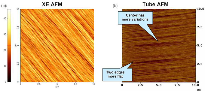
Figure 6. Images of a hard disk surface taken by a (a) Park Systems’ AFM and by a (b) conventional piezoelectric tube based AFM.
The immediate advantage of the zero background curvature in the Park AFM is demonstrated in the defect review analysis of a hard disk surface. Figure 6 shows images of a hard disk surface acquired by a Park Systems’ Park AFM as shown in Figure 6 (a) and a piezoelectric tube based AFM as shown in Figure 6 (b). Both images came from a comparison study in real fab condition by the same hard disk industry client. The images are obtained after deglitching those lines due to door opening & closing in the fab facility as shown in Figure 7. Note the striking difference between the two in Figure 6. The image taken by the piezoelectric tube based AFM is processed by a line-by-line curvature flattening, and one can clearly notice the distortion in the image as a result of the curvature flattening. The two edges look more flat, and the center has more variation. As pointed out earlier, a tube scanner has quite a bit of background curvature, approximately 80 nm over 15 μm scan. Since the current image by the piezoelectric tube based AFM is about 10 μm in scan size, it would have a significant background curvature. Without the curvature flattening, the image would be so curved to the point that one cannot even see the line features on a hard disk. Even with the curvature flattening, the nanoscale features on the hard disk would undoubtedly get distorted due to the high order fitting from the flattening process. Making matters worse, the door deglitching adds to the distortion as it is impossible to fit correctly both the glitches and the background curvature. The RMS roughness from such data is bound to be wrong.
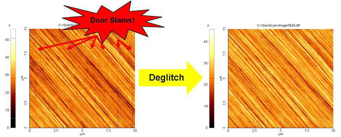
Figure 7. The deglitching of a hard disk surface image taken by Park Systems AFM. The glitches are generated when a door is closed or opened in the actual fab facility of a hard disk industry client. Note that the door glitches are removed without affecting the texture of the original raw data.
The image acquired using a Park Systems AFM correctly reflects the texture of the original sample. As the background curvature remains absolute minimum, the removal of door glitches is the only correction to be made, and it can be easily implemented without using high order fitting and changing the original raw image data as shown in Figure 7.
Pole-Tip-Recession (PTR) 1 : True Non-Contact AFM vs. Tapping AFM
The density of information on a hard disc drive depends on the distance between the read-and-write head of a hard-disk drive. Usually the head is floating on an air cushion that builds up between the rotating hard-disk plate and the read-and-write head that “flies” at a distance to the hard disk of several nanometers. The active parts for read-and-write action are two ferritic poles that guide and focus the magnetic field close to the disk as shown in Figure 8. The pole-tip recession (PTR) is the difference in height between the pole tip material and the air-bearing surface (ABS). As one way of increasing the storage density in rigid disk drives, many efforts were taken to minimize the head-media gap, and consequently resulted in signal loss;4,5 the pole tip had to be recessed as little as possible, only to the point of preventing damage by contact with the disk. For this reason, the nano-metrology of PTR is a critical task6 with significant economic impact.
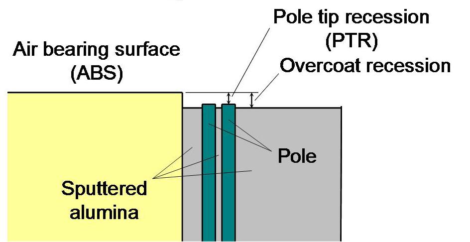
Figure 8. The pole-tip-recession (PTR) of a hard disk drive is the difference in height between the pole tip material and the air-bearing surface (ABS). The image is a cross section of a typical thin film head showing the pole tips, undercoat/overcoat, gap, and the air bearing surface (ABS).
Since the reference plane (ABS) is far from the pole tip, the small height of PTR is easily buried in the background curvature of the piezoelectric tube scanner, which is more than ten times larger than the PTR height.9, 10 It gets even worse when the images taken with piezo tube based AFMs are line-by-line flattened with high order polynomial fitting. The background curvature poses a significant bottleneck in the PTR metrology. As the pole tip region has a typical height of a few nanometers and a width of 50 mm, the resulting background curvature these AFMs would be a few hundred nanometers over the scan range of 50 mm.
Figure 9 shows a flattened image taken by a piezoelectric tube based AFM using tapping mode. First, note the residual background curvature even after line-by-line flattening. Since there are air-bearing surfaces at the sides, the average is flat, but the inside, recessed region, looks curved upward. That’s the major problem with image processing, since you do not know if the curvature is coming from the original surface, from a scanner artifact, or from the sly image processing.
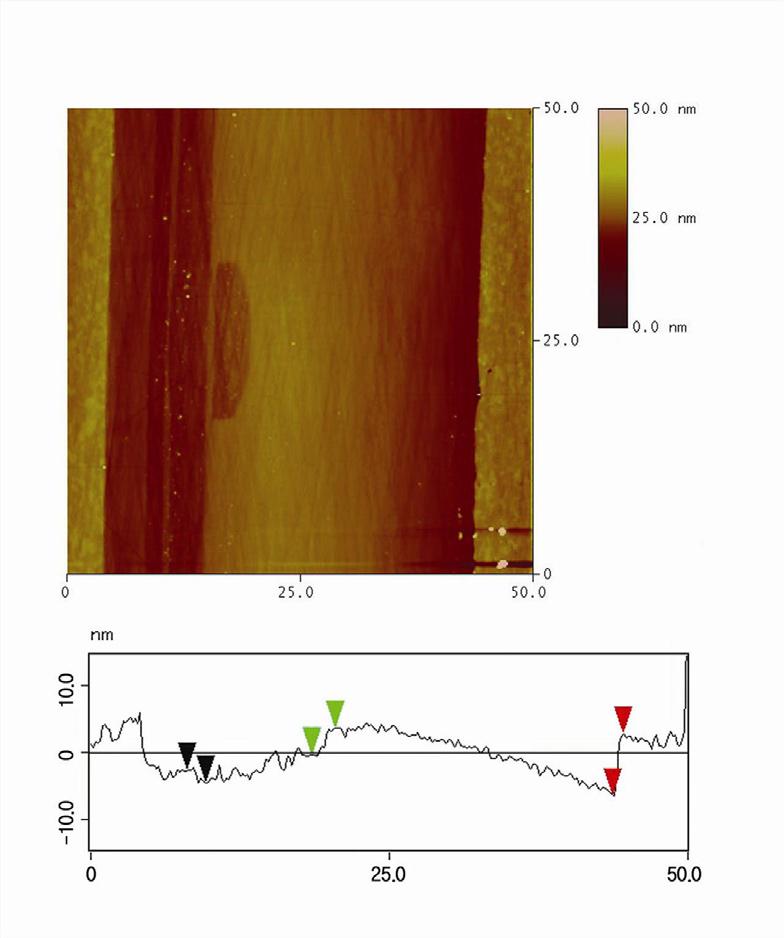
Figure 9. Image of the pole-tip region taken by a piezoelectric tube scanner based AFM in tapping mode. The background curvature is similar to the height change in the pole tip area.
There is an even more pressing issue of tapping force changing the PTR morphology in conventional piezoelectric tube based AFMs. Note that the pole-tip (the half moon shaped area with two vertical stripes on its left) in the PTR image by the piezoelectric tube based AFM is located lower than its surroundings, contrary to the design as shown in Figure 8. Here, we have found that the tapping mode AFM can cause serious artifacts due to the tapping force because the pole-tip is made of softer materials and the tapping force depresses the pole tip more than its surroundings and generate incorrect PTR values.
In tapping mode, as stated in the original paper, the tip is made to strike the surface on each oscillation with sufficient oscillation amplitude and energy to overcome the stickiness of the surface.11 In other words, the tip depresses the sample surface by striking on it at each oscillation cycle. If the sample is homogeneous, the overall depression would not change the topography. However, if the sample is composed of various materials, the tapping force will depress the soft areas more than the harder areas. This phenomenon will not be obvious if the thickness of different materials is small, or if the sample surface is not smooth. However, in the case of PTR, this effect is prominent since the sample surface is very flat, and each material has large thickness.
In order to verify this, we performed Force Modulation Microscopy (FMM). As shown in Figure 10, the pole tip area appears much darker than its surrounding, which means the pole tip is much softer than its surrounding. This is in accordance with the material properties of the pole tip, made of permalloy, and its surrounding, made of alumina.
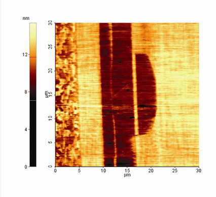
Figure 10. Force Modulation Microscopy (FMM) image showing local variations in surface stiffness.
Figure 11 shows an unprocessed raw data of the same sample taken with Park Systems’ Park AFM in True Non-Contact AFM mode. As shown in the line profile of Figure 11, the recessed region is completely flat with raised Air Bearing Surfaces (ABS) at both sides. Moreover, the pole tip area is located higher than its alumina coated region, as was designed to be. This conclusively demonstrates the superiority of the Park AFM performance especially in its zero background curvature and True Non-Contact AFM.
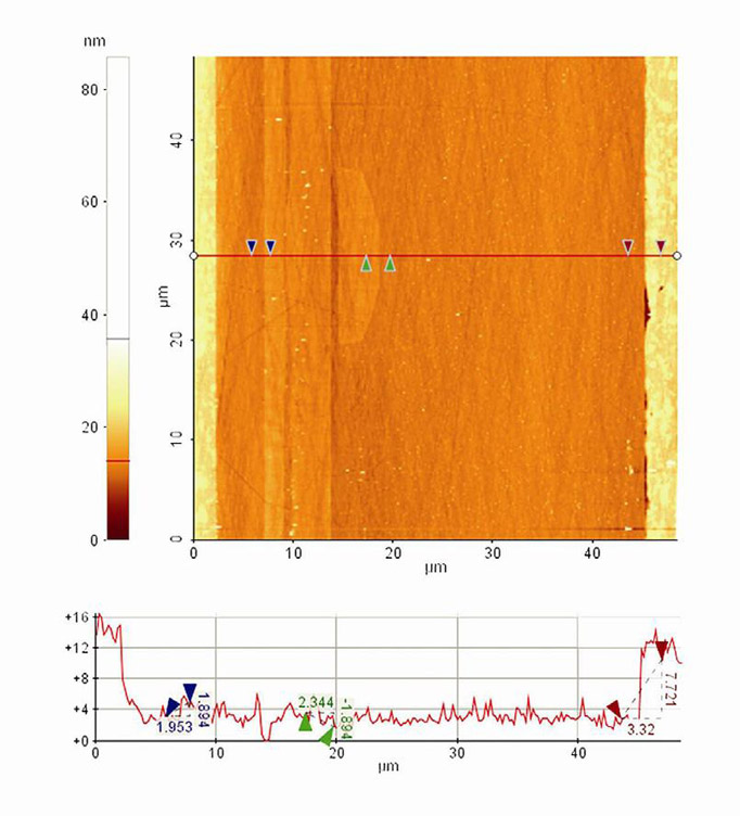 Figure 11. PTR region imaged with Park Systems’ Park AFM in True Non-Contact AFM mode. The image shows no background curvature.
Pole-Tip-Recession (PTR) 2: Two Height Peaks in ABS Area.
As shown in Figure 8, the ABS area is used as a reference plane for the subsequent measurements of the PTR. Therefore, the accurate reference height of the ABS area is critical in performing more rigorously and reliably characterizing the PTR. In Figure 12, the histogram of the ABS area image taken by Park Systems’ Park AFM clearly shows two peaks. The peaks are separated by about 1.65 nm. This simply reflects what we see optically in the ABS area, i.e., dark and bright regions. Two regions have obviously different heights. Please note that the distinction of the two height peaks in the ABS area is an important measure of an AFM performance in itself. Conventional piezoelectric tube based AFMs cannot distinguish the two height peaks since such nano-metrological differentiation is impossible due to the intrinsic background curvature and subsequent flattening.
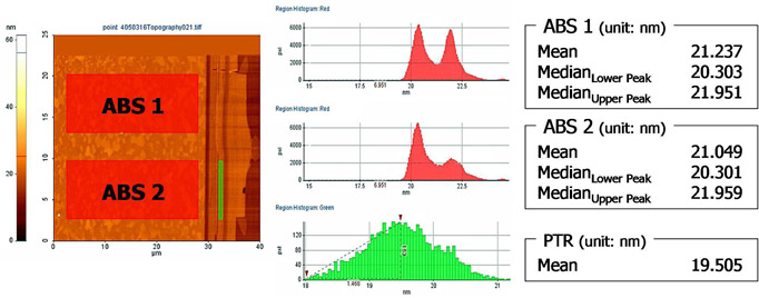
Figure 12. The histograms of two ABS and one PTR areas whose images are taken by Park Systems’ AFM. In other words, the mean value of heights in ABS area will change depending on the size and location of selected areas. However, the median values of the two peaks will remain the same regardless of the size and location of selected ABS areas.
The averaged value of heights in a given ABS area will change by the distribution of dark and bright regions in the area. In other words, the mean value of heights in ABS area will change depending on the size and location of selected areas. However, the median values of the two peaks will remain the same regardless of the size and location of selected ABS areas. If one can distinguish two height peaks in a given ABS area, median values of the ABS area represent more accurate, more reliable, and more consistent reference height for PTR characterization.
Conclusion
It is apparent that old AFMs based on piezoelectric tube scanners are not suitable in hard disk metrology due to their scanner’s artifacts. We also noticed that the tapping mode can not only cause a serious amount of damage to the PTR, but also change the relative height measurements between regions of different materials. Moreover, there is always the undeniable fact that tapping causes faster tip damage compared to True Non-Contact. Whether in defect review or in PTR metrology, the zero background curvature and True Non-Contact mode of the Park AFM are found to be critical in the accurate and reliable metrology of the hard disk industry.
References
1. V. Ashok et al., IEEE Trans. Mag. 36, 2736 (2000).
2. Martin Smallen, and Jerry J. K. Lee, Trans. ASME 115, 382 (1993).
3. J. Kwon et al., Rev. Sci. Instrum. 74, 4378 (2003).
4. W. Scott et al, J. Appl. Phys. 87, 6182 (2000).
5. W. Scott, and B. Bharat, J. Appl. Phys. 91, 8328 (2002).
6. C. Nadimpalli, F.E. Talke, Tran. ASME 117, 580 (1995).
7. D. Zipperian, Datatech (1996) pp. 163-168.
8. D. Zipperian, and Dallas Meyer, IDEMA insight (Jan./Feb. 1999) pp. 8-11.
9. K. Babcock, and P. Hopkins, Datatech (1996) pp. 155-160.
10. K. Babcock, and P. Hopkins, IDEMA insight (Jan./Feb. 1997) pp. 7-8.
11. Q. Zhong, D. Inniss, K. Kjoller, and V. B. Elings, Surf. Sci. Lett. 290, L688 (1993).