


Stabilizing the piezoresponse for accurate and crosstalk-free ferroelectric domain characterization via dual frequency resonance tracking
Ilka Hermes1, Romain Stomp2
1Park Systems Europe, Mannheim, Germany
2Zurich Instruments, Zurich, Switzerland
INTRODUCTION
Due to their unique electromechanical and electrical properties, ferroelectrics found widespread industrial application, e.g. as actuators, sensors and capacitors[1], [2]. Nowadays, researchers investigate the suitability of ferroelectrics for modern communication technology such as 5G[3], as active layers in photovoltaics [4], [5], and many more[6].
Ferroelectricity is the result of a change in crystal symmetry during a phase transition. Here, an off centering of the center ion or a tilting of ionic groups introduces a spontaneous electrical polarization. To lower the electrostatic energy the crystal forms domains of parallelly aligned polarization. Without external electric field, these domains are oriented randomly, so that the macroscopic electrical polarization of the crystal remains zero (Figure 1a). However, electric fields can switch the domain orientation permanently, which allows customizing domain patterns for specific applications (Figure 1b).[7]
The characterization of the resulting domain patterns requires an electromechanical imaging technique that locally visualizes domains with high spatial resolution to respond to ever decreasing device sizes. Here, Piezoelectric Force Microscopy (PFM), a contact mode Atomic Force Microscopy (AFM) method, is ideally suited[8], [9]. In PFM, a conductive tip attached to a cantilever scans the surface of a ferroelectric sample, while applying an AC voltage between the tip and a back electrode below the sample. Since all ferroelectric materials are piezoelectric, the applied AC voltage introduces a periodic deformation of the sample, called piezoresponse (Figure 1c). For domains with a polarization perpendicular to the sample surface, the piezoresponse is either in phase or 180° out of phase with the applied AC voltage, depending on the polarization orientation in the domains below the tip (Figure 1d). Therefore, the PFM phase carries information on the domain orientation. Meanwhile, at the position of boundaries between adjacent domains of opposite polarization orientation, so called domain walls, the piezoresponse cancels out and the PFM amplitude reaches a minimum. Therefore, the PFM amplitude visualizes the position of domain walls[8].
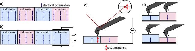
Figure 1: a) Schematic of ferroelectric domains with parallel electric polarization (small blue arrows). The random formation of + and –domains cancels out a macroscopic polarization. b) The application of a local electric field selectively switches the orientation of a –domain to a +domain. c) PFM work principle: an AC voltage applied between tip and a conductive back electrode below the sample introduces an oscillating piezoresponse (red double arrow) in the ferroelectric. The cantilever detects the oscillating piezoresponse via the optical beam deflection method. d) Depending on the domain orientation below the tip the material either expands or contracts, leading to 180° phase shift between oppositely oriented out of plane domains.
In its standard configuration, PFM applies low frequency AC voltages, far from the contact resonance of the cantilever. This technique, called single frequency off resonance PFM, has an intrinsically low sensitivity for topographic crosstalk caused by contact mechanics between tip and surface on the PFM signal. Depending on the samples, off resonance PFM may require high amplitudes of the AC voltages to achieve a sufficient signal to noise ratio in the piezoresponse. For materials with weak piezoresponses, like thin films, or materials sensitive to high drive voltages, the signal-to-noise ratio can be enhanced by applying an AC voltage close or at the contact resonance of the cantilever, which is approximately three to five times the free resonance[8]. Yet, in this single frequency resonance enhanced PFM technique the detected piezoresponse becomes prone to crosstalk, e.g. from topography and sample mechanics. The frequency of the contact resonance strongly depends on a stable and unchanged tip sample contact, which is difficult to achieve while scanning, particularly on rough surfaces. Furthermore, heterogeneities in the sample mechanics introduce additional changes in the contact resonance[10].
Here, we demonstrate how to stabilize the resonance enhanced piezoresponse by using an additional feedback that tracks the contact resonance during the PFM scan in a technique called Dual Frequency Resonance Tracking (DFRT) on a Park Systems NX10 AFM with a Zurich Instruments HF2 Lock In Amplifier (LIA). For DFRT, the HF2 generates two sidebands left and right of the contact resonance at frequencies given by the bandwidth at half maximum of the contact resonance. During the PFM scan, the feedback continuously compares the amplitudes of both sidebands and readjusts the frequency of the AC voltage to keep the amplitude ratio constant[10]. Due to the number of available demodulators and feedbacks, the HF2 allows the simultaneous tracking of the vertical contact resonance (CR1) and the lateral resonance (CR2) as illustrated in Figure 2. At the same time, the simple access to the vertical and lateral measurement signals as well as the possibility to apply an external tip bias directly to the cantilever on the Park Systems NX series allow for a straight forward synchronization of the AFM and the LIA. The PFM signals can be fed into the NX AFM controller via the five available auxiliary inputs and displayed and recorded by Park Systems’ SmartScan™ software or by the data acquisition module of Zurich Instruments’ LabOne® software.
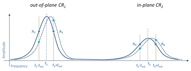
Figure 2: Frequency spectrum of cantilever in contact showing the vertical contact resonance CR1 and lateral contact resonance CR2. The sidebands used for the resonance tracking are generated at frequencies fm (grey bars) from the contact resonances, given by the bandwidth of the respective resonance. A feedback monitors the amplitude ratio of both sidebands (A2 and A3 for the vertical resonance and A5 and A6 for the lateral resonance) and readjusts the frequency of the AC voltage to keep the ratio constant.
For this application note, we imaged the piezoresponse on a Bismuth Ferrite (BFO) film via DFRT and compared the results to a single frequency resonance enhanced PFM measurement. We found a significant reduction of topographic crosstalk for DFRT in both PFM amplitude and PFM phase, leading to a clear visualization of domain walls and oppositely oriented domains, respectively. Additionally, we conducted simultaneous vertical and lateral DFRT PFM measurements, illustrating the technique’s versatility and potential for reliable and accurate domain imaging on ferroelectric materials.
Experimental
For the DFRT PFM measurement on the ferroelectric BFO, we used a Park Systems NX10 coupled with a Zurich Instruments HF2 LIA. All measurements were conducted with a conductive PtIr coated PPP EFM cantilever with a nominal spring constant of 2.8 N/m and a free resonance of 75 kHz. With a free resonance of 75 kHz, we expect a vertical contact resonance in the range of 250 400 kHz and a lateral contact resonance in the range of 550 750 kHz. We chose a setpoint of ~30 nN for all scans. The scan rate was 0.2 Hz, the resolution 512×512 px and the scan size 2×2 µm.
For the vertical DFRT and single frequency resonance-enhanced PFM measurements, we gave the vertical cantilever displacement from the signal access module to the first input of the HF2, while applying the tip bias via the HF2 output 1 directly to the cantilever via a conductive clip type probehand. The PFM signals were fed from the HF2 to the AFM controller via the four auxiliary outputs in the HF2 and four auxiliary inputs on the NX AFM controller. Thereby, the required PFM signals could be displayed and recorded via SmartScan™ by choosing the internal contact or PFM mode and adding the according auxiliary inputs to the measurement channels. If the collection of additional signals was required, we could readily synchronize the AFM scan and data collection by connecting the end of line trigger from the AFM controller to the DOI of the HF2 and enable the data acquisition via LabOne®.
For the simultaneous lateral and vertical DFRT PFM measurements, we gave the vertical cantilever displacement to input 1 and the lateral cantilever displacement to input 2 of the HF2. Both the vertical and the lateral AC voltage frequency could be applied to the cantilever via output 1, by adding the lateral drive from output 2 to the vertical AC drive.
Results and Discussion
For the demonstration of DFRT PFM on a Park Systems NX10 AFM with a Zurich Instruments HF2 LIA, we imaged the ferroelectric domains of a BFO sample. Prior to our first measurement of the vertical piezoresponse of BFO, we set up the frequency feedback by recording the frequency spectrum of the AC voltage (1 V) during tip-sample contact. We observed the vertical contact resonance at 353 kHz. With a bandwidth at half maximum of 4.4 kHz, we generated the sidebands at ±2.2 kHz from the resonance, at 350.8 and 355.2 kHz, respectively (Figure 3). Generally, a symmetric shape of the contact resonance ensures a stable operation of the DFRT feedback; we found deviations from a symmetric resonance at higher voltages, possibly due to electrostatic interactions. With the appropriate frequencies for center and sideband frequencies, as well as the pixel dwell time for the scan, the feedback advisor in Zurich Instruments’ LabOne® software found suitable gain settings for the measurement.
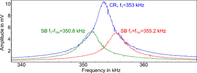
Figure 3: Frequency spectrum of the AC voltage between tip and sample in contact, with AC amplitudes of 1 V on the carrier signal and both sidebands. The vertical contact resonance (CR1) was positioned at 353 kHz, both sidebands (SB) were generated in 2.2 kHz from the contact resonance.
The results of vertical DFRT PFM measurement are summarized in Figure 4. The imaged BFO sample had a root mean square roughness of 3.4 nm with distinct holes, up to 20 nm in depth (Figure 4a). These topographical features were barely visible in the PFM signals (Figure 4b and c), indicating a well functioning DFRT feedback, which compensates for topographic crosstalk caused by changes in the tip sample contact mechanics. Indeed, the frequency signal of the DFRT feedback (Figure 4d) imaged frequency shifts at positions corresponding to the holes in the height channel. To further illustrate the minimized topographic crosstalk in the PFM signals, we extracted line profiles along the red line for each of the signals. The profiles showed that the hole in the height channel, highlighted by the blue boxes in the images and the line profiles, had little influence on the PFM amplitude and no influence on the PFM phase. Instead, we observed a clear domain wall and domain orientation contrast in PFM amplitude and PFM phase, respectively. The minima in the PFM amplitude correlated to the outlines of the domains in the PFM phase, which captured the full 180° contrast, indicative of oppositely oriented out of plane domains.
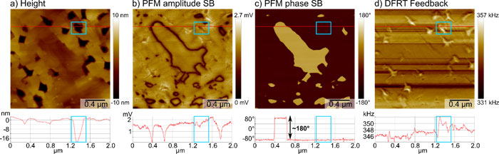
Figure 4: Results of vertical DFRT PFM measurement on a BFO sample. a) Sample topography in the height channel with line profile extracted along the red line. Exemplary hole outlined by blue box in image and profile. b), c) PFM amplitude and phase measured on the second sideband (SB) at f1+f1m with an amplitude of 1 V, resolving the position of the domain walls and the domain orientation, respectively. The line profiles extracted along the red line show amplitude minima at the domain walls and a full 180° phase contrast, as well as minimal topographic crosstalk (blue box). d) Frequency signal of the DFRT feedback imaged the compensated frequency shifts introduced by holes in the topography (blue box).
To compare the DFRT measurement to a single frequency resonance enhanced PFM measurement, we conducted another measurement at the same sample location with the same measurement parameters, but without DFRT feedback (Figure 5). Here, we measured the PFM signals at a frequency close to the contact resonance with 1 V AC excitation. The height channel in Figure 5a resolved the same holes as the previous scan - one exemplary hole outlined by the blue box. However, in this measurement we could clearly observe crosstalk caused by the holes in the PFM amplitude as well as the PFM phase (Figure 5b and c). Besides the domain walls, the PFM amplitude now featured the holes in the topography as amplitude minima. Without previous knowledge of the domain structure, a distinction of topographic crosstalk and a true PFM signal is difficult. Likewise, the PFM phase showed phase extrema at the position of the holes in the topography in addition to a ~180° domain contrast. The phase contrast caused by the topographic crosstalk was up to 120° and could easily lead to errors in the data interpretation.
Additionally, we recorded three frequency spectra with the same cantilever, 1 V AC amplitude and the same loading force (~30 nN) at three different locations in the measurement area (Figure 5d). We found a significant shift in the vertical contact resonance for the second of the recorded spectra by almost 10 kHz. This shift in the contact resonance between three consecutive spectra perfectly illustrates the importance of tracking the resonance frequency for resonance enhanced PFM.
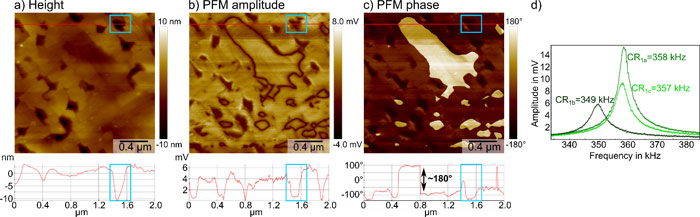
Figure 5: Vertical single frequency resonance-enhanced PFM measurement on the same BFO sample location as the previous DFRT PFM measurement, with the sample height in a), the PFM amplitude in b) and the PFM phase in c). The measurement was conducted with 1 V AC amplitude at 356 kHz for a contact resonance of 357 kHz. The PFM amplitude and PFM phase resolved the position of domain walls as amplitude minima and the domain orientation with a full 180° phase contrast, respectively. Both PFM signals displayed a strong topographic crosstalk (blue boxes). d) Three consecutive frequency spectra with 1 V AC amplitude at three different locations in the measurement area showing a 9 kHz shift in the vertical contact resonance (CR1).
Finally, we tested the capabilities for simultaneous vertical and lateral DFRT PFM. We used the two inputs on the HF2 to feed the vertical and the lateral cantilever displacement from the NX10 AFM into the LIA and gave the AC excitation voltage at the vertical and the lateral resonance directly to the cantilever. The frequency spectra of the vertical contact resonance at 350 kHz (1 V AC amplitude) and the lateral contact resonance at 690 kHz (1 V AC amplitude) are displayed in Figure 6a and b. Analog to the first DFRT measurement, we determined the frequencies of the two sidebands according to the bandwidth at half maximum of both resonances. For the vertical signal, the sidebands were at ±2 kHz from the contact resonance; for the lateral signal, the sidebands were at ±1.5 kHz from the contact resonance. To track both resonance frequencies independently during the scan, we used two frequency feedbacks to track the vertical as well as the lateral resonance. To find the appropriate feedback gains, we used the advisor function in the LabOne® software.
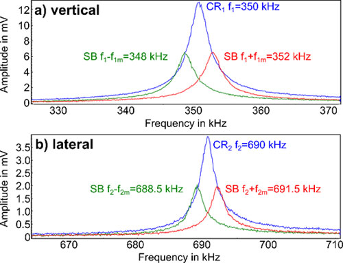
Figure 6: Frequency spectra of the AC voltage between tip and sample in contact, with AC amplitudes of 1 V on the carrier signal and both sidebands. a) The vertical contact resonance (CR1) was at 350 kHz, both sidebands (SB) were generated in 2 kHz from the CR1. b) The lateral contact resonance (CR2) was at 690 kHz, both SB were generated in 1.5 kHz from CR2.
Figure 7a shows the sample topography on the same sample location as both previous measurements (Figure 4 and 5), resolving a comparable surface structure with distinct holes. The vertical PFM amplitude strongly resembled the signal in Figure 4, with a clear domain wall contrast, visible as amplitude minima (Figure 7b). We observed minimal crosstalk with the topography, indicating a well functioning DFRT feedback in agreement with the previous DFRT PFM measurement (Figure 4). The lateral PFM amplitude in Figure 7c, on the other hand, showed a vastly different structure than the vertical PFM amplitude. Here, a periodic amplitude contrast resolved in plane ferroelastic twin domains of BFO, suggesting a successful lateral DFRT PFM measurement[11].
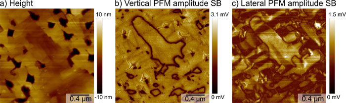
Figure 7: Results of a simultaneous vertical and lateral DFRT PFM measurement on a BFO sample. a) Sample topography in the height channel. b), c) Vertical and lateral PFM amplitude, respectively. Both were measured on the second sideband (SB) at f1+f1m and f2+f2m with an amplitude of 1 V. The vertical PFM amplitude resembled previous results by imaging the position of the domain walls with minimal topographic crosstalk. The lateral PFM amplitude resolved characteristic periodic ferroelastic domains.
Conclusion
In this study, we successfully imaged ferroelectric domains of a Bismuth Ferrite (BFO) film with resonance enhanced Piezoelectric Force Microscopy (PFM) on a Park Systems NX10 Atomic Force Microscope (AFM) with a Zurich Instruments HF2 Lock In Amplifier (LIA). We could show that the additional frequency feedback in Dual Frequency Resonance Tracking (DFRT) significantly reduces topographic crosstalk compared to single frequency resonance enhanced PFM. Thereby, DFRT PFM generates more reliable and accurate PFM data for the characterization of ferroelectric domain patterns, required for the industrial application of ferroelectrics, as well as academic research. Especially on rough samples, DFRT compensates for shifts in the contact resonance introduced by changes in the tip sample contact mechanics. Furthermore, we demonstrated the capability of simultaneous vertical and lateral DFRT PFM measurements highlighting the technique’s versatility and potential in material characterization. The readily accessible measurement signals on AFMs from Park Systems allow for a simple implementation and synchronization of the AFM and Zurich Instruments’ HF2 LIA for DFRT PFM.
Acknowledgement
We like to thank Dr. Akash Bhatnagar, Centre for Innovation Competence SiLi-nano® Germany, for providing us with the BFO sample.
REFERENCES
[1] D. Damjanovic, P. Muralt, and N. Setter, “Ferroelectric sensors,” IEEE Sens. J., vol. 1, no. 3, pp. 191–206, 2001.
[2] P. Muralt, “Ferroelectric thin films for micro-sensors and actuators: a review,” J. Micromech. Microeng., vol. 10, no. 2, pp. 136–146, 2000.
[3] N. M. Dawley et al., “Targeted chemical pressure yields tuneable millimetre-wave dielectric,” Nat. Mater., vol. 19, no. 2, pp. 176–181, 2020.
[4] A. Bhatnagar, A. Roy Chaudhuri, Y. Heon Kim, D. Hesse, and M. Alexe, “Role of domain walls in the abnormal photovoltaic effect in BiFeO3,” Nat. Commun., vol. 4, no. 1, p. 2835, 2013.
[5] K. T. Butler, J. M. Frost, and A. Walsh, “Ferroelectric materials for solar energy conversion: photoferroics revisited,” Energy Environ. Sci., vol. 8, no. 3, pp. 838–848, 2015.
[6] J. F. Scott, “Applications of Modern Ferroelectrics,” Science, vol. 315, no. 5814, pp. 954–959, Feb. 2007.
[7] A. K. Tagantsev, L. E. Cross, and J. Fousek, Domains in ferroic crystals and thin films, vol. 13. Springer, 2010.
[8] E. Soergel, “Piezoresponse force microscopy (PFM),” J. Phys. D Appl. Phys., vol. 44, no. 46, p. 464003, 2011.
[9] P. Güthner and K. Dransfeld, “Local poling of ferroelectric polymers by scanning force microscopy,” Appl. Phys. Lett., vol. 61, no. 9, pp. 1137–1139, 1992.
[10] B. J. Rodriguez, C. Callahan, S. V Kalinin, and R. Proksch, “Dual-frequency resonance-tracking atomic force microscopy,” Nanotechnology, vol. 18, no. 47, p. 475504, 2007.
[11] A. Alsubaie, P. Sharma, J. H. Lee, J. Y. Kim, C.-H. Yang, and J. Seidel, “Uniaxial Strain-Controlled Ferroelastic Domain Evolution in BiFeO3,” ACS Appl. Mater. Interfaces, vol. 10, no. 14, pp. 11768–11775, 2018.