


-
fifber FM_KPFM CopperFoil PtfeMembrane Conduct tip_bias_mode SurfaceOxidation TemperatureControllerStage Polypropylene UnivOfMaryland PolyStylene LeakageCurrent OxideLayer Electical&Electronics Chloroform cooling Magnetic Solar CrossSection PECurve LithiumNiobate single_layer University_of_Regensburg semifluorinated alkane MfmPhase #EC thermal_conductivity Indium_tin_oxide NUS_NNI_Nanocore GranadaUniv rubber AIN CompactDisk AnodizedAluminumOxide Copolymer
Report image
If you found this image unacceptable, please let us know. We will review your report and take action if we determine this image is really unacceptable.
Taegeuk Mark Lithography on PZT
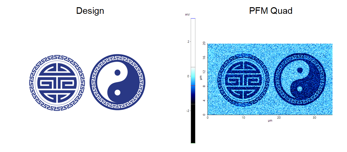
Re-arranged the domain pole direction on PZT surface using bias mode of lithography.
Scanning Conditions
- System: NX10
- Scan Mode: Lithography
- Cantilever: PPP-ContScPt (k=0.2N/m, f=25kHz)
- Scan Size: 35μm×20μm
- Scan Rate: 0.5Hz
- Pixel Size: 1024 × 1024
- Tip Bias: 10V for patterned area
- Scan Mode: Lithography
- Cantilever: PPP-ContScPt (k=0.2N/m, f=25kHz)
- Scan Size: 35μm×20μm
- Scan Rate: 0.5Hz
- Pixel Size: 1024 × 1024
- Tip Bias: 10V for patterned area