


-
frequency_modulation NUS_NNI_Nanocore Grain Sphere Sapphire IRDetector HighAspect ChemicalCompound Ecoli alkanes Optoelectonics WS2 SICM Beads ConductiveAFM Layer Lift Hexatriacontane StyreneBeads FloppyDisk Phosphide PolymerBlend PyroelectricDetector CarbonNanotube Vac MultiferroicMaterials Magnets TyphimuriumBiofilm Chemical Vapor Deposition margarine ConductingPolymer thermoplastic_elastomers Granada SiliconCrystal SSRM
Report image
If you found this image unacceptable, please let us know. We will review your report and take action if we determine this image is really unacceptable.
ITO Film Sputter Deposited onto Silicon
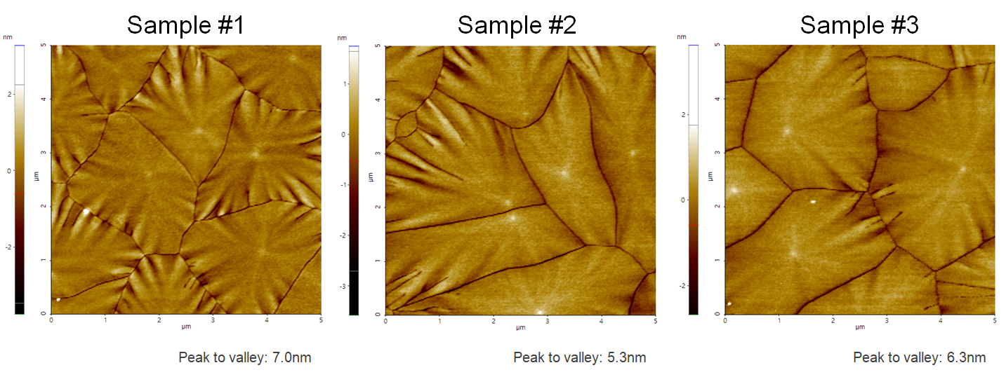
ITO-film, which was sputter deposited onto silicon. The grain size of those samples was influenced by changing the process settings in the Cluterline RAD sputter deposition system, one of the deposition tool platforms manufactured by Evatec.
Scanning Conditions
- System: NX10
- Scan Mode: Non-contact
- Cantilever: PPP-EFM (k=2.8N/m, f=75kHz)
- Scan Size: 5μm×5μm
- Scan Rate: 0.1Hz
- Pixel Size: 256 × 256
- Scan Mode: Non-contact
- Cantilever: PPP-EFM (k=2.8N/m, f=75kHz)
- Scan Size: 5μm×5μm
- Scan Rate: 0.1Hz
- Pixel Size: 256 × 256