


-
Sidewall Insulator Moire Defects ForceDistanceSpectroscopy Materials Phthalocyanine PinpointNanomechanicalMode Roughness StrontiuTitanate GaN Vinylpyridine NeodymiumMagnets phase_change Conducting molecule Display Polypropylene conductive epitaxy NanoLithography chemical_compound Fet ThermalConductivity TiO2 Reading OpticalWaveguide Heating DIWafer TipBiasMode Floppy GaAs Boundary optoelectronics EFMAmplitude
Report image
If you found this image unacceptable, please let us know. We will review your report and take action if we determine this image is really unacceptable.
Polymer patterns on Si (2/2)
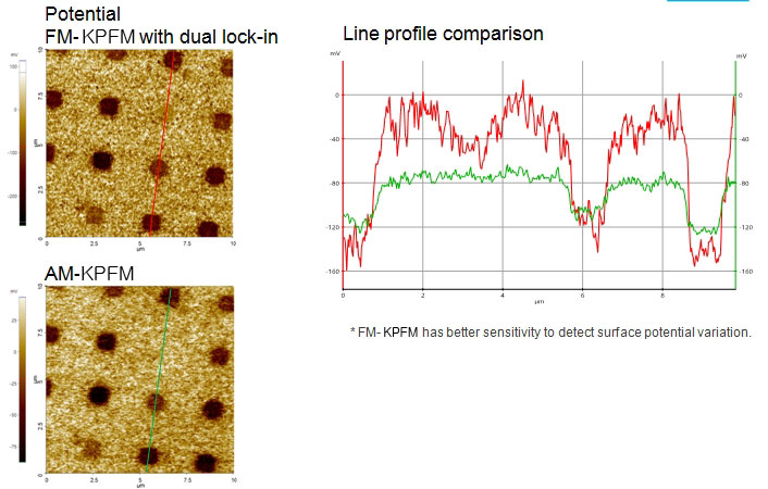
Scanning Conditions
- System: NX10
- Scan Mode: KPFM
- Cantilever: NSC36Cr-Au (k=1N/m, f=90kHz)
- Scan Size: 10μm×10μm
- Scan Rate: 0.2Hz
- Pixel: 512×256