


-
INSP Workfunction bias_mode Vanadate AIN Metal dichalcogenide LateralForce INSPParis VinylAlcohol PetruPoni Fiber DIWafer BismuthFerrite frequency_modulation LFM Leakage Force-distance ScanningSpreadingResistanceMicroscopy ScanningIon-ConductanceMicroscopy Tapping Steps C_AFM nanobar HighResolution KPFM HexacontaneFilm Transparent PS_LDPE conductive MonoLayer hetero_structure semifluorinated alkane Polytetrafluoroethylene phase_change
Report image
If you found this image unacceptable, please let us know. We will review your report and take action if we determine this image is really unacceptable.
Multi-layer necking device defect
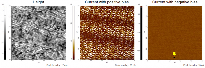
Scanning Conditions
- System : NX-Wafer
- Scan Mode: C-AFM
- Scan Rate : 2Hz
- Scan Size : 2μm×2μm
- Pixel Size : 512×256
- Cantilever : AD-2.8-AS (k=2.8N/m, f=75kHz)