


-
Oxidation AlkaneFilm TCS Materials self_assembly OxideLayer Regensburg Device PS_PVAC Semiconductor Solar Cross-section INSPParis Permalloy LightEmission cross section mono_layer Indent GaP TemperatureControllerStage MechanicalProperty Hafnium_dioxide Pzt non_contact small_scan temperature_control Gold TemperatureControl AM_KPFM Polyimide bias_mode ElectrostaticForceMicroscopy UTEM LiquidCrystal HighAspect
Report image
If you found this image unacceptable, please let us know. We will review your report and take action if we determine this image is really unacceptable.
Semiconductor device, W-plug
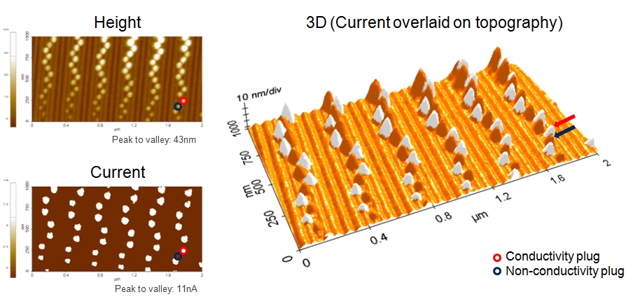
Scanning Conditions
- System: NX10
- Scan Mode: Conductive AFM
- Cantilever: ElectriMulti75-G (k=3N/m, f=75kHz)
- Scan Size: 2μm×1μm
- Scan Rate: 0.3Hz
- Pixel: 512×256
- Sample bias: +1V