


-
BiFeO3 SRAM P3HT LateralForce Mechanical&nanotechnology Conducting Film IcelandSpar BFO India Heating ElectroChemical DentalProsthesis PinpointNanomechanicalMode self-assembled_monolayer Temasek_Lab ContactModeDots Lateral_Force_Microscopy TyphimuriumBiofilm PolycrystallineFerroelectricBCZT GlassTemp PFM cannabinoid Array SiliconeOxide Vacuum membrane BreastCancerCell Tungsten SurfaceOxidation Cobalt-dopedIronOxide dichalcogenide Ito Ferrite Granada
Report image
If you found this image unacceptable, please let us know. We will review your report and take action if we determine this image is really unacceptable.
Monolayer Graphene on PDMS Surface
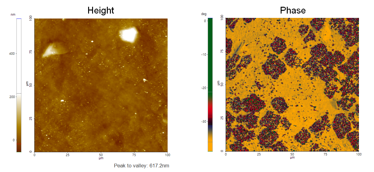
Monolayer Graphene grown on Cu foil using CVD process is transferred on to PDMS substrate.
Scanning Conditions
- System: NX20
- Scan Mode: Tapping
- Cantilever: Access-NC (k=113N/m, f=330kHz)
- Scan Size: 100μm×100μm
- Scan Rate: 0.6Hz
- Pixel Size: 256 × 256
- Scan Mode: Tapping
- Cantilever: Access-NC (k=113N/m, f=330kHz)
- Scan Size: 100μm×100μm
- Scan Rate: 0.6Hz
- Pixel Size: 256 × 256