


-
MfmAmplitude Ram Glass ContactModeDot ULCA Electrical&Electronics semifluorinated alkane Lattice India UnivMaryland HanyangUniv Sidewall Vac Led ChemicalCompound GaAs PiezoelectricForceMicroscopy pinpoint mode cross section LiquidCrystal ThermalConductivity Silver PolymerBlend SmallScan Sphere Techcomp Annealing membrane molecules Chloroform NusEce CuSubstrate dielectric trench Lateral Silicon
Report image
If you found this image unacceptable, please let us know. We will review your report and take action if we determine this image is really unacceptable.
MoS2 Layers on SiO2
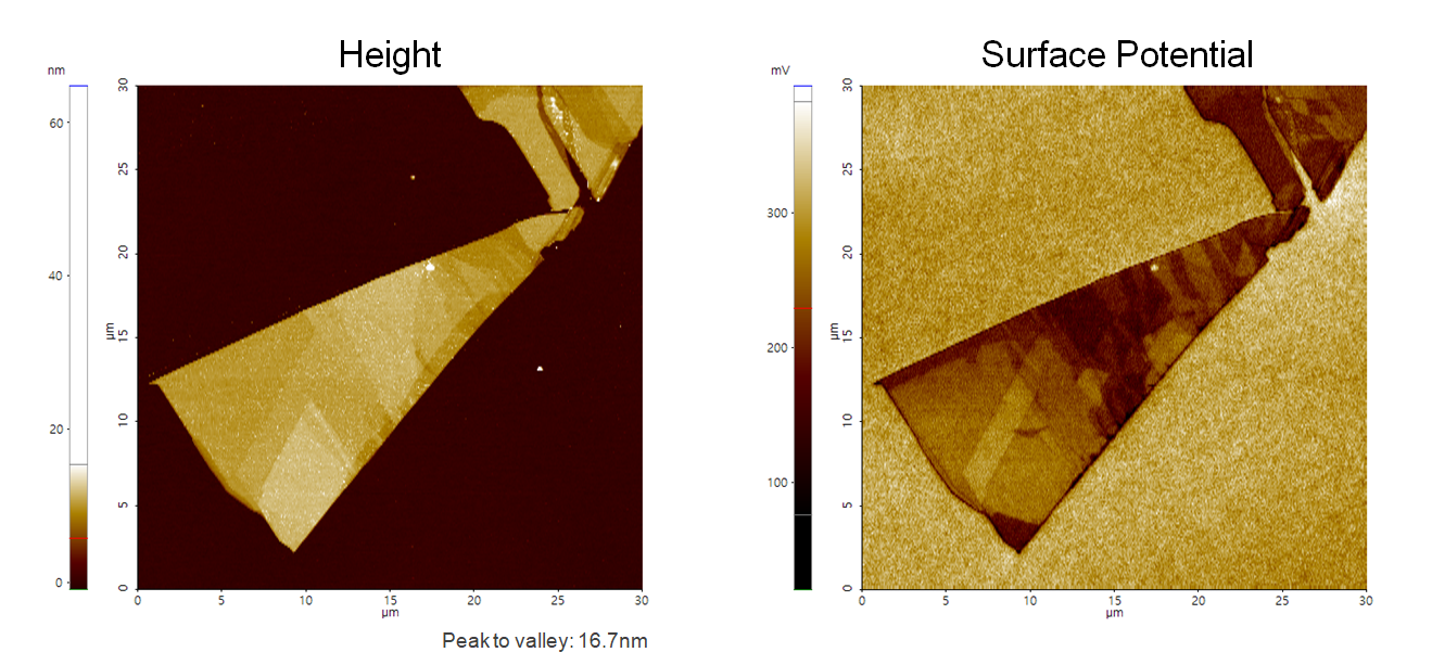
A few layers of MoS2 on SiO2
Scanning Conditions
- System: NX10
- Scan Mode: AM-KPFM
- Cantilever: NSC36Cr-Au B (k=2N/m, f=130kHz)
- Scan Size: 30μm×30μm
- Scan Rate: 0.3Hz
- Pixel Size: 512 × 256
- Scan Mode: AM-KPFM
- Cantilever: NSC36Cr-Au B (k=2N/m, f=130kHz)
- Scan Size: 30μm×30μm
- Scan Rate: 0.3Hz
- Pixel Size: 512 × 256