


-
AIN domain_switching Flake Etch Polyvinylidene GaP WPlug CuSubstrate Dr.JurekSadowski HexagonalBN semifluorinated_alkanes Nanopattern light_emitting LateralPFM Piranha Conductivity Magnetic Force Microscopy Laser Pyroelectric Melt HACrystal Monisha Materials FrictionalForce Self-assembledMonolayer Thermal Pattern Topography Writing SFAs CNT Device Inorganic SoftSample RedBloodCell
Report image
If you found this image unacceptable, please let us know. We will review your report and take action if we determine this image is really unacceptable.
ITO Film Sputter Deposited onto Silicon
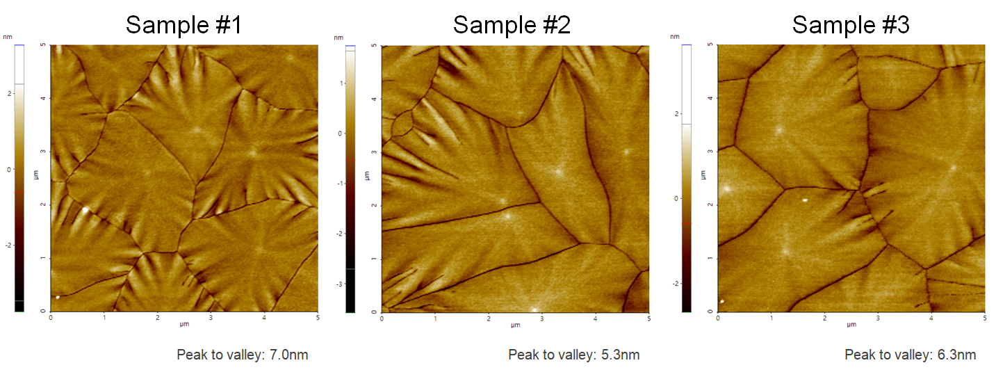
ITO-film, which was sputter deposited onto silicon. The grain size of those samples was influenced by changing the process settings in the Cluterline RAD sputter deposition system, one of the deposition tool platforms manufactured by Evatec.
Scanning Conditions
- System: NX10
- Scan Mode: Non-contact
- Cantilever: PPP-EFM (k=2.8N/m, f=75kHz)
- Scan Size: 5μm×5μm
- Scan Rate: 0.1Hz
- Pixel Size: 256 × 256
- Scan Mode: Non-contact
- Cantilever: PPP-EFM (k=2.8N/m, f=75kHz)
- Scan Size: 5μm×5μm
- Scan Rate: 0.1Hz
- Pixel Size: 256 × 256