


-
Anneal #EC NanoLithography PvdfBead Hexylthiophene PMNPT Monisha MfmPhase cannabidiol Kevlar LaAlO3 CntFilm Polypropylene BiVO4 PinPointMode Tin disulfide SrO SelfAssembly VortexCore lithography AdhesionEnergy Piezoelectric PECurve Cell 2d_materials Reading VerticalPFM Sio2 ULCA Defects fe_nd_b Liquid Corrosion P3HT Pipette
Report image
If you found this image unacceptable, please let us know. We will review your report and take action if we determine this image is really unacceptable.
Atomic steps on GaP(Gallium Phosphide) layer on Si
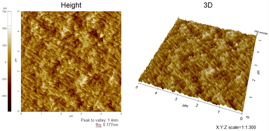
Scanning Conditions
- System: NX20
- Scan Mode: Non-contact
- Cantilever: PPP-NCHR (k=42N/m, f=300kHz)
- Scan Size: 5μm×5μm
- Scan Rate: 1Hz
- Pixel: 512×512