


Piezoresponse force microscopy (PFM) is a functional Atomic force microscopy (AFM) mode, which probes electromechanical material properties on the nanometer scale in addition to the sample topography. As a conductive tip scans the surface in contact, an AC voltage introduces an electromechanical response in piezoelectric compounds and thereby resolves local variations of piezoelectric and ferroelectric properties. PFM has gained increasing recognition for the unique information it can offer on the electromechanical coupling characteristics of various materials including actuators, sensors, and capacitors for modern communication technology. Common applications of PFM include:
• local characterization of electromechanical properties of ferroelectric materials, including detailed domain mapping and study of domain switching dynamics, visualized in the material’s ferroelectric hysteresis;
• testing of micro- and nanoelectromechanical devices (e.g., piezoelectric actuators, transducers, and MEMS), electro-optical devices and nonvolatile memory components (i.e., FeRAM devices) by addressing their reliability issues such as electromechanical imprint, fatigue, and dielectric breakdown;
• exploring the local and global relationship between ferroelectric polarization and other material properties on novel polymer and bio-engineered materials based on detailed nanoscale structural and electromechanical characterization.
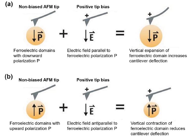
Figure 1. Fundamental principle of PFM, ferroelectric domains with (a) downward polarization and (b) upward polarization.
This mode note introduces the basics, instrumentation, and potential exemplary applications of PFM. Various topics are discussed, including improvement of image quality and resolution, elimination of artifacts and extraction of information from PFM images, as well as piezoresponse force spectroscopy, which allows quantitative analyses of the piezoelectric material response under applied voltage. In PFM, a conductive AFM tip is brought into contact with the surface of ferro- or piezoelectric materials, and a pre-set voltage is applied between the sample surface and the AFM tip. The voltage establishes an external electric field within the sample. Due to the inversed piezoelectric effect present in ferroor piezoelectric materials, the sample locally expands or contracts according to the direction of the electric field. For example, if the electrical polarization of a ferroelectric domain below the tip is oriented perpendicular to the sample surface and parallel to the applied electric field, the domain will experience a vertical expansion as shown in figure 1 (a). Since the AFM tip is in contact with the sample surface, this domain expansion bends the AFM cantilever upwards and increases the deflection. Conversely, if the initial domain polarization is antiparallel to the applied electric field, the domain will contract, which leads to a decreased cantilever deflection as shown in figure 1 (b). Therefore, the change of the cantilever deflection offers information on the direction and relative magnitude of the ferroelectric polarization of the domain below the tip.
However, the static change of domain dimensions is typically in the picometer range. To increase the signal-to-noise ratio PFM applies an AC voltage to the conductive material coated tip. This AC voltage results in a surface oscillation with the same frequency as the applied AC voltage. If the sample domain polarization is oriented parallel to the applied electric field, the piezoelectric sample response will be in-phase with the excitation. If the domain polarization is oriented anti-parallel to the applied electric field, the response will be out-of-phase with the excitation, as shown in figure 2. Thus, the phase-contrast between two oppositely oriented vertical domains is 180°. The amplitude and phase of the sample oscillation are directly detected as deflection signal of the AFM cantilever, which is in contact with the surface, and read out via the lock-in amplifier.
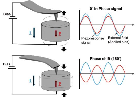
Figure 2. Schematic of PFM working principle: An AC voltage between the sample and the conductive cantilever introduces a periodic piezoelectric response of the sample. Depending on the polarization orientation of the domain below the tip, the piezoresponse signal is in phase or 180° out-of-phase with the excitation.
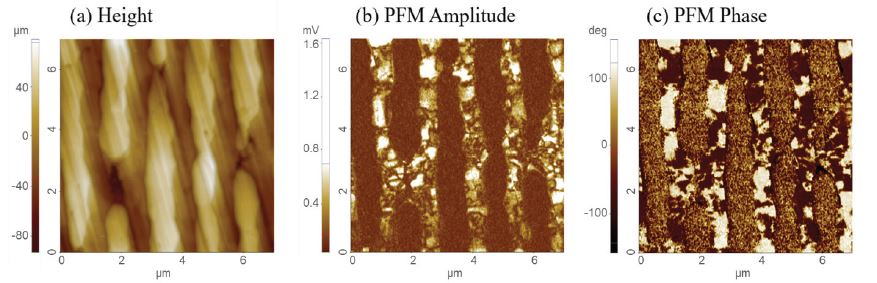
Figure 3. PFM amplitude and phase images with height information.
In PFM imaging, the phase contrast between AC excitation and the sample’s piezoelectric response directly relates to the polarization orientation of the domain below the tip. The amplitude of the piezoelectric response on the other hand resolves the position of domain walls. Here, the signal gets minimal since the response of two domains with opposite polarization orientation and 180° phasecontrast cancels out. Figure 3 shows PFM amplitude and phase images as well as height image on a multilayer ceramic capacitor sample. The PFM signals are well presented when +2V tip bias is applied. The cantilever type is PPP-EFM (k = 2.8 N/m and f = 75 kHz), scan size, pixel resolution and scan rate are 7 μm × 7 μm, 256 × 256 and 0.2 Hz, respectively.
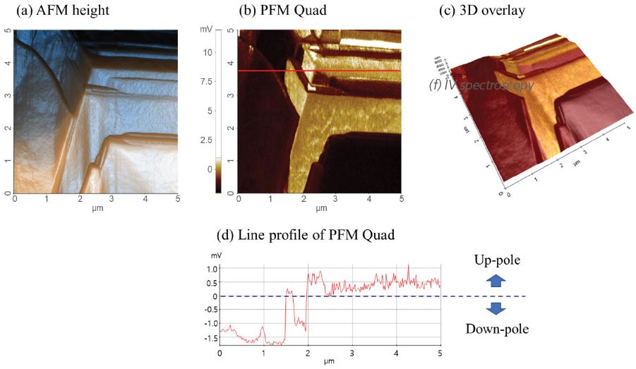
Figure 4. AFM topography (a) and PFM quad image (b) of BaTiO3 sample surface. 3D overlay (c) with the PFM quad color is overlaid on 3D surface morphology, and line profile of PFM quad image (d) which shows domain polarization direction. Image courtesy: Biomedical engineering,Yeditepe University, Turkey
Figure 4 shows an example of PFM quad, which is a combination of PFM amplitude and phase, obtained on a composite barium titanate (BaTiO3) sample. As can be observed in PFM quad image, clear contrast is displayed depends on material type, which is hardly recognized by height image.
For samples, that contain domains with out-of-plane and in-plane orientations, not only components perpendicular to the surface in contact with the AFM tip, but also components along different directions within the surface plane, vector PFM with vertical and lateral channels can provide more complete information as shown in figure 5. The out-of-plane polarization is estimated by tracking the vertical cantilever deflection, the vertical PFM signal, and the in-plane polarization can be determined from the lateral torsion of the cantilever, the lateral PFM signal. Using both the vertical and lateral PFM information, a more detailed and complete electromechanical response analysis is achieved. Figure 5 shows the vertical and lateral piezoresponse on a bismuth ferrite sample (BiFeO3).
Besides domain imaging, PFM offers insights into ferroelectrics switching properties and dynamics via piezoresponse force spectroscopy, which measures the local PFM response as an additional DC bias between tip and sample surface is swept. The polarity of the local ferroelectric domain below the tip aligns according to the applied voltage depending on the sign and magnitude of the voltage. Figure 6 shows the hysteresis loop of PFM amplitude vs. DC voltage and PFM phase vs. DC voltage on a lead zirconate titanate (PZT) thin film. This phase hysteresis loop reveals the change of the polarization direction with the applied DC voltage. As the voltage gradually increases, the domain appears to be reversed by approximately 180° at 0.8 V and 3.1 V, respectively. In piezoresponse force spectroscopy, the user can perform an array of PFM signal vs. voltage spectroscopy measurements at various locations. The spectroscopy provides information on local switching behavior of ferroelectric domains.
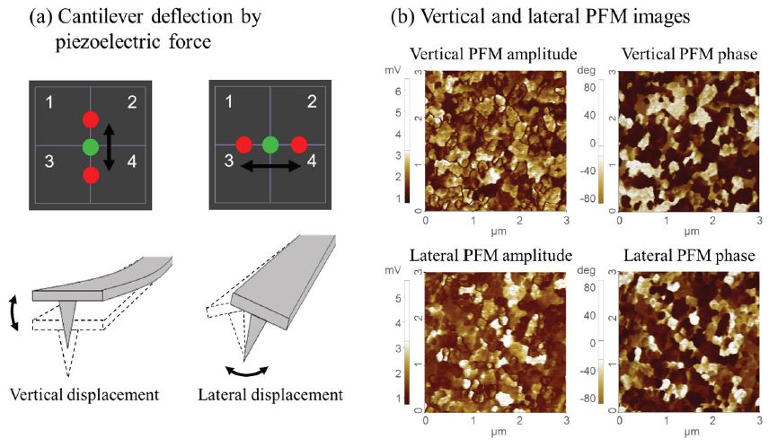
Figure 5. Schematic view of vertical and lateral cantilever deflection and torsion due to an out-of-plane and in-plane piezoresponse signal, respectively in (a). Vertical and lateral PFM amplitude and phase images on a bismuth ferrite (BiFeO3) sample.
On ferroelectric samples, PFM can be combined with Nanolithography (see “Nanolithography mode note” for more information) to tailor customized domain patterns on the nanometer scale. Here, the application of positive or negative DC voltages to the tip can change the polarization of vertical ferroelectric domains by 180°. Figure 7 shows the Nanolithography PFM capability on a PZT film surface by writing the Park Systems logo via DC bias application and a subsequent PFM scan to image the logo on the PFM amplitude and phase. To write the logo on the ferroelectric surface +10 V tip bias was applied to the dark areas of the lithography design in figure 7 (a) and -10 V was applied to the bright areas of the design to switch the domain orientation in the opposite direction for the background of the logo. After writing the domain pattern on the PZT film, the PFM amplitude clearly imaged the domain walls, while the PFM phase showed the opposite domain orientations between the Park Systems logo and the background in figure 7 (b) and (c).
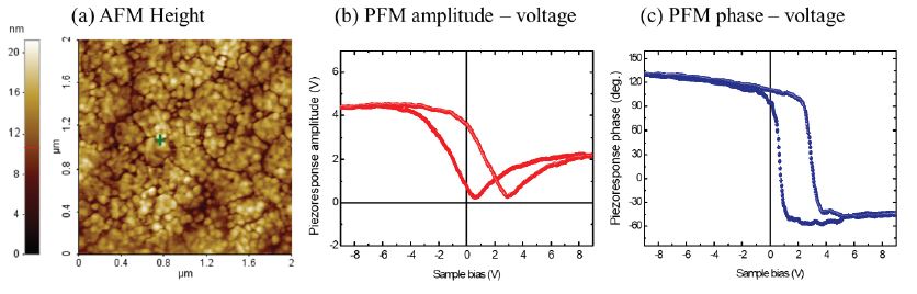
Figure 6. Representative piezoresponse force spectroscopy on PZT film sample to locally measure the ferroelectric hysteresis curve. AFM height of PZT film with greed cross indicating the position of the spectroscopy measurement in (a), PFM amplitude vs. voltage curve (b), and PFM phase vs. voltage curve (c).
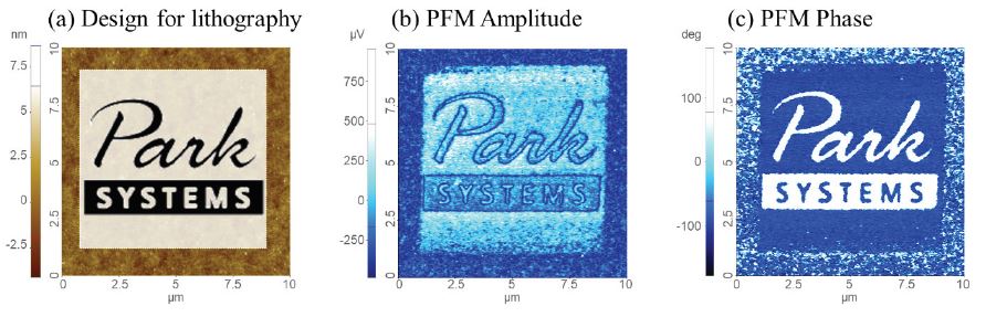
Figure 7. Nanolithography design on a PZT thin film for domain formation via ferroelectric switching in (a). During the writing, a positive +10 V DC bias is applied in the dark areas and a negative -10 V bias is applied in the bright areas of the design. PFM amplitude in (b) and phase in (c) after switching the domains according to the design.