


 PinPoint™ Nanomechanical acquires images simultaneously and in real-time by taking the high speed force-distance curves when the XY scanner stops, while maintaining well defined control of contact force and contact time between the tip and the sample
Santa Clara, CA November 05, 2014
Park Systems, a leading manufacturer of atomic force microscopy (AFM) products, announces PinPoint™ Nanomechanical Mode a new application designed to measure and map mechanical properties in materials and biological cells simultaneously and in real-time from high speed force-distance (F-d) curves with accurate control of both contact force and time. This new feature is compatible with Park AFM products Park NX10, Park NX20 and Park NX-Bio used world-wide for unparalleled accuracy in AFM imaging for industry and research. This new feature for AFM is applicable to many materials especially polymers and will provide valuable data for cell imaging in many bio research applications.
"PinPoint™ Nanomechanical mode was designed for failure analysis engineers, researchers in materials science, and cell biologists who use F-d spectroscopy or force modulation mode to characterize the mechanical differences of material components or cells in their samples in less time in the orders of magnitude and with more accuracy," explains Keibock Lee, Park Systems President. "We continue to develop applications and products to advance our equipment to ever increasing levels of precision which is what makes Park AFM imaging the world leader in nanoscale imaging."
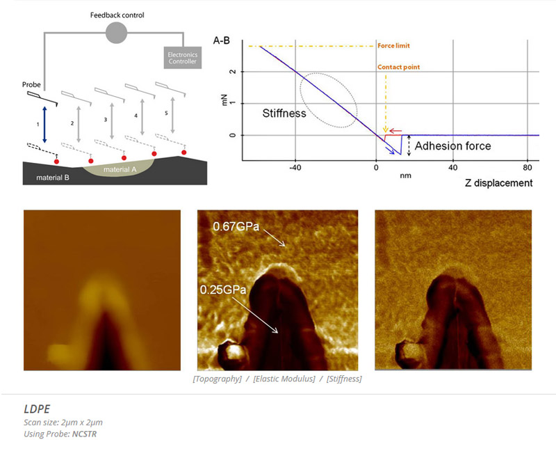
By adjusting contact force and time, PinPoint™Nanomechanical identifies embedded details of sample material under its surface and characterizes topography, stiffness, elastic modulus, adhesion force, and adhesion in materials. PinPoint™ Nanomechanical mode acquires images simultaneously and in real-time by taking the high speed force-distance curves when the XY scanner stops, while maintaining well defined control of contact force and contact time between the tip and the sample.
"In the past, taking an extensive force volume imaging over an area took a prohibitively long amount of time. For example, 32×32 pixel force volume imaging would take a few hours and an AFM scan at 256×256 pixels would take over thirty hours," comments Lee. "PinPoint ™Nanomechanical allows users to get even more accurate and detailed data in real time using existing Park AFM equipment."
Using PinPoint™ Nanomechanical Mode makes it possible to study the variation and position of mechanical properties across a surface at previously unattainable resolutions using a non-destructive tip mode that controls the peak normal force and minimizes the lateral force on the probe. One of the advantages is achieving truly quantitative material property mapping with the resolution and convenience required in today's complex nanotechnology environment. By adjusting contact force and time, PinPoint™ Nanomechanical imaging can reveal embedded details of material components on and under the sample surface, enabling a distribution map of material components in a high resolution of nanometer scale and analysis comparing with a surface morphology directly.
The new PinPoint™ mode acquires AFM Nanomechanical property maps of stiffness, elastic modulus and adhesion force on a sample surface simultaneously with topography from high speed Force-distance curve at each point. The process is done using Park Systems's unique methodology, while measuring a morphology of the sample, the XY scanner stops at each data acquisition point for taking the high speed force-distance curves with well defined control of contact force(or distance) and contact time between the tip and the sample. This makes evaluation of mechanical properties in materials a seamless operation for material science professionals, creating reliable analysis at vastly improved levels of speed and accuracy.
For more information, please go to: http://www.parkafm.com/index.php/park-afm-modes/nanomechanical-modes
About Park Systems
Park Systems is a world-leading manufacturer of atomic force microscopy (AFM) systems with a complete range of products for researchers and industry engineers in chemistry, materials, physics, life sciences, and semiconductor and data storage industries. Park's products are used by over a thousand institutions and corporations worldwide. Park's AFM provides highest data accuracy at nanoscale resolution, superior productivity, and lowest operating cost thanks to its unique technology and innovative engineering. Park Systems, Inc. is headquartered in Santa Clara, California with its global manufacturing, and R&D headquarters in Korea. Park's products are sold and supported worldwide with regional headquarters in the US, Korea, Japan, and Singapore, and distribution partners throughout Europe, Asia, and America.
Please visit http://www.parkafm.com or call 408-986-1110 for more information.