


Patterned arrays of magnetic nanostructures have become one of the key issues in recent years because of its potential application to information technology with respect to magnetic storage devices. Particular attention has been given to the magnetic properties of periodic arrays of micron and submicron elements of very different shapes, especially dots and stripes. The study of these arrays of submicron elements is the basis for the development of magnetic memories and nanopatterned recording media, since the inter-element interaction determines the integration limits of magnetic memories and nanopatterned recording media.
The periodic magnetic domain structure was observed by using a magnetic force microscopy (MFM). The method was the first scanning probe technique and turned out to be a powerful tool for submicron-scale magnetic image mapping. In order to measure the magnetic properties of periodic structures based on magnetic/nonmagnetic films, the MFM technique is better suited that possess the high sensitivity required to monitor magnetic domain structure in thin films and very small elements of different shapes.
We fabricated two-dimensional (2D) Co magnetic arrays by the photolithography with KrF laser source and the wet etching (Transene Inc., TFB) process. A Co film, 40 nm thick, was deposited on a 6-inch Si(100) wafer by using a sputtering system.
The magnetic domain structure has been investigated using a MFM system, which is basically a scanning probe microscopy (Park SYSTEMS, XE-100) equipped with a magnetic tip (Nanosensors, PPP-MFMR). Also, the MFM system was equipped with an electromagnet, which allows us to investigate the evolution of the magnetic domains in an in-plane applied magnetic field.
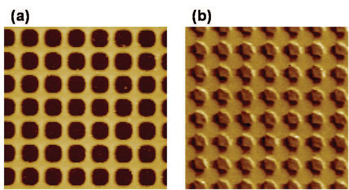
FIG. 1: (a) AFM and (b) MFM images of 2D patterned arrays of Co antidot structures. The scan area is 10 μm x 10 μm.
Figure 1 shows the atomic force microscopy (AFM) and the MFM images obtained from 2D patterned arrays of Co antidote structures. The MFM image in Fig. 1(b) has three different domains. Two are wedge-shaped domains connecting the holes and the other is a diamond-shaped domain. For the wedge-shaped domains, the magnetization vector is parallel to the connecting boundaries at the holes and points from dark to bright inside the domain. The magnetization vector in the diamond-shaped domain is oriented along the diagonal. This configuration minimizes the magnetostatic energy.
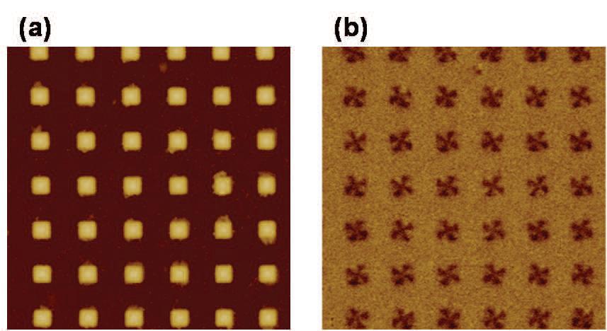
FIG. 2: (a) AFM and (b) MFM images of 2D patterned arrays of Co dot structure. The scan area is 10 μm x 10 μm.
As shown in Fig. 2(a), the AFM image study reveal that a 2D patterned arrays of submicron square dot structures was fabricated. The AFM image clearly shows a square-lattice pattern with a periodicity of about 1.6 μm. By comparing the AFM and the MFM images [see Fig.2(a) and Fig. 2(b), respectively], it is clear that the topography and the magnetic contrast are well separated. The MFM image of the square pattern shown in Fig. 2(a) demonstrates a Landau-Lifshitz-type flux closure domain structure with 90° domain walls and a central vortex. The magnetic charges are mainly concentrated along the domain walls. In systems with a negligible magnetocrystalline anisotropy, the balance of demagnetization and exchange energies results in flux-closure structures such as four fold-closure-domain pattern in thin squares. It can be seen that, apart from the contrast associated with domain walls, the one related to the vortex core is also clearly detected.
As seen in Fig. 3, two kinds of vortex chirality appear in all the patterned arrays, namely clockwise and counter-clockwise, with an approximately equal probability due to the two fold energy degeneracy. This finding reveals the bistability of magnetic vortices and the statistically random distribution of vortex chirality. Additionally, the vortices of different chiralities present clearly the corresponding MFM images under an applied field.
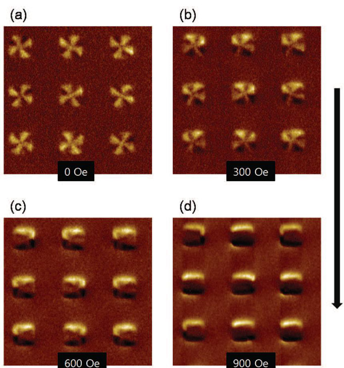
FIG. 3: Field-dependent MFM images of square Co dots. The scan area is 5 μm x 5 μm .
The field-dependent MFM images show that the application of the field (indicated by a black arrow) induces the domain-wall motions (see Fig. 3). The intersection moves, first, perpendicular to the applied field direction and gradually approaches the corner. At H = 300 Oe, the field increases the size at the expense of the right (or left) domain. As the strength of applied field keeps increasing, the magnetization vectors are antiparallel to the external field, and eventually all the magnetic moments are reversed and become parallel to the field. As seen in Fig. 3(d), the magnetic domains gradually collapse with each other. These characteristics are closely related to the distribution of vortex annihilation (nucleation) fields.


