


General Considerations
Nitride-based semiconductor materials (i.e., GaN, InGaN, AlN) have attracted considerable attention in the past years for their applications to electronic and optoelectronic devices, including blue/green light emitting diodes (LEDs), laser diodes (LDs), and solid state transistors.1 Researchers have long known of the properties of the group-III nitrides, including their wide bandgaps and robust nature, but had not been able to find a suitable substrate on which to grow thin films of these compounds. To be practical, the substrate needed a crystalline structure that matched GaN (utilized as standard n/p-type contact) and it had to be available in large sizes at a reasonably low cost. Recent advancements in the epitaxial thin film growth techniques and substrate material selections partially addressed this problem. However, the lattice parameters of sapphire, the substrate of choice for most LED manufacturers, are not an exact match to GaN (16% lattice mismatch), which results in a high density of crystalline defects (i.e., dislocations, point defects) 2 SiC is better suited as a substrate material, but is still very costly and also generates stacking mismatch boundaries in the device structure, which significantly shorten the device lifetime. Large area Si substrates (4”, 6” and beyond) are rapidly becoming the substrate of choice for electronic device manufacturers, however substrate mismatch effects are still present and a high degree of surface cracking (due to the built-in strain) occurs when the critical film thickness is surpassed. In addition, Si substrates are less resistant from a mechanical standpoint when compared to both sapphire and SiC.
To further enhance the brightness of blue/green LEDs grown by metal organic chemical vapor deposition (MOCVD), most of the established manufacturers in the Asian region (Japan, Korea, Taiwan, and China) have adopted surface patterning techniques for both (a) the sapphire to epitaxial film interface (sapphire substrate patterning achieved by substrate preparation techniques) and (b) epitaxial film to fabricated contact interface (p‑side roughening achieved by MOCVD epitaxial growth methods). These methods, if properly designed and implemented, allow for a more efficient coefficient of light extraction from the LED device to be achieved.3 For both patterning cases, proper information concerning the surface morphology is vital to achieving target requirements. Most of the traditional microscopy techniques (i.e., optical microscopy, scanning electron microscopy, etc.) have been found to have major limitations in terms of applicability to monitoring the above mentioned surface roughening techniques. Included are spatial resolution limitations, sample preparation techniques, reliability and reproducibility issues, amount of time spent to collect data and so on. Atomic force microscopy (AFM) offers a simple, efficient, and non‑destructive alternative to investigating the various types of patterns achievable for both sapphire substrate and top LED surface cases.
Traditional AFM tools have been designed with the core of the scanning mechanism relying on an XYZ piezoelectric tube scanner. As such, crosstalk and nonlinearity were inherently built in this design. The Park AFM scan system, which has been developed by Park Systems decoupled the XY and Z-scanners and was introduced as the next generation AFM design. As a result, the True Non-Contact mode was enabled.
Park AFM System Overview
For all products of the Park AFM, the Z-scanners controlling the vertical movement of the probe tip, which is fundamental to acquiring the surface morphology information, is completely decoupled from the XY-scanner, which moves the sample in the XY directions. This fundamental architectural design change provides the user with significant operational advantages enabling the True Non-Contact mode. Physical separation of the XY and Z-scanners allows for complete removal of the background curvature and effectively eliminates the crosstalk and nonlinearity issues that are intrinsic to conventional piezoelectric tube based AFM systems. This uniquely designed Park AFM scan system not only increases the data collection speed by at least 10× compared to conventional piezoelectric tube scanners, but also minimizes the error due to the inherent nonlinearity of the scanner itself.
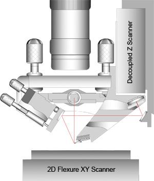
Figure 1. Cross-section view of Park AFM’s scanning system. Perfectly decoupled XY-Z scanner enables independent movement of Z scanner, which makes True Non-Contact scanning with optimal feedback speed.
The Park AFM scan system is a core feature that gives the competitive edge to the Park AFMs. Park Systems’ innovative scanner design separates the Z-scanners from the XY-scanner, enabling exceptional Z-servo performance, orthogonality, and scan accuracy. (See Figure 1.) The Z-scanners, which controls the vertical movement of the AFM tip and is fundamental to acquiring the surface morphology information, is completely decoupled from the XY-scanner which moves a sample in X and Y horizontal directions. From the structure, Park AFMs remove background curvature from a fundamental standpoint, and effectively eliminates the crosstalk and nonlinearity problems that are intrinsic to conventional piezoelectric tube based AFM systems. The Z-scanners is designed to have a higher resonant frequency than conventional piezoelectric tube scanners. For this reason, a stacked piezoelectric actuator is used for the Z-scanners with a high push-pull force when appropriately pre-loaded. Since the Z‑servo response of the Park AFM scan system is very accurate, the probe can precisely follow the steep curvature of a sample without crashing or sticking to the surface.
In the Park AFM scan system, the XY-scanner is a Body Guided Flexure scanner, which is used to scan a sample in the X and Y directions only. The flexure hinge structure of the XY-scanner guarantees highly orthogonal 2D movement with minimum out-of-plane motion. The 2D flexure stage of the Park AFM scan system has only 1 nm ~2 nm of out-of-plane motion for the scan range of 50 μm, compared to the inherent 80 nm by the piezoelectric tube scanner of conventional AFMs over the same scan range. (See “Technology behind the Park AFM” for detail.) The symmetrical flexure scanner design also makes possible to place much larger samples on the sample stage than could normally be accommodated by a piezoelectric tube scanner. Furthermore, the symmetry enables to keep the scanner balanced even when a sample is loaded, so that the dynamics of the XY-scanner is not distorted by the sample holder and/or the loaded sample. Since the flexure scanner only moves in the XY direction, it can be scanned at much higher rates (10 Hz ~50 Hz) than would be possible with a standard AFM. The Park AFM not only achieves a structural design innovation that yields a trend setting AFM performance, but it also brings state-of-the-art improvements to the electronics. The Park AFM Control Electronics incorporates advanced digital circuitry with precision software and hardware components that empower high speed and high capacity data processing, which are designed to enable the scanner, the core unit of the AFM, to provide efficient, accurate and fast control, and to facilitate the acquisition of stable images even beyond a scan speed of 10 Hz. Besides the high speed measurement ability, Park AFM’s electronics controls the movement of the AFM system precisely by the closed-loop scan system, which is indispensable to map each additional property to the very point of enhanced topographic details. Even though an AFM system can acquire data with multiple modes, unless the system displays the exact position of measurement, it needs software correction (or calibration) to map the data on the exact position. Correction by software remapping usually works well when the imaging area is comparatively small, but closed-loop scan is applicable on any imaging area without distortion.
Patterned Sapphire Substrates (PSS) Investigation
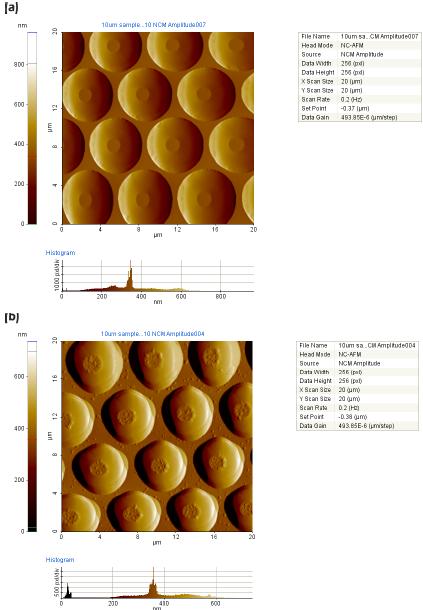
Figure 2. Surface morphology at the 20 μm scale of two different patterned sapphire substrate samples (a) smooth dome surfaces and clean areas between domes and (b) both dome top surfaces and areas between domes show damage and/or residue. Images were acquired with an XE-150 AFM instrument in True Non-Contact mode at 0.2 Hz with 256 pixel resolution.
Shown in Figures 2 are AFM surface topography images (True Non-Contact mode, amplitude channel) at the 20 μm scale of two different types of patterned sapphire substrates (PSS) specimens acquired utilizing an XE-150 manufactured and commercialized by Park Systems. Circular features (i.e., domes) are noticeable with diameters ~ 5 μm and about 1.7 μm in height independent on the scan axis direction. Although the patterns were manufactured by the same method for both cases, the material in Figure 2 (a) displays smooth, featureless dome surfaces with clean areas between these domes, while the sample in Figure 2b shows a certain amount of surface damage and/or residue for both top dome and areas in between. Figure 3 represents corresponding AFM surface topography views (Tapping Mode, amplitude channel) at the 20 μm scale of the same PSS samples (as shown in Figure 2) acquired utilizing a piezoelectric tube scanner instrument manufactured and distributed by a different vendor. Several image discrepancies are easily noticeable between Figures 3 and 2. As such, in Figures 3,
• The features appear to be cylindrical (to some extent elongated along the slow axis scan).
• Features heights are ~ 1.5 μm along the fast scan axis (X) and in the 1.1 ~ 1.4 μm range along the slow scan axis (Y).
• No significant differences are noted in areas between the features of these two samples.
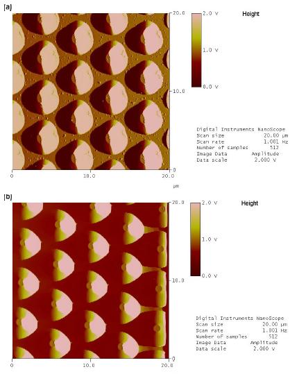
Figure 3. Surface morphology at the 20 μm scale of the same two patterned sapphire substrate samples shown in Figure 2. The images show (a) asymmetrical features (somewhat elongated along the slow axis scan) with clean areas between the features and (b) asymmetrical shape features displaying damage and/or residue in the areas in between. These images were acquired with a conventional piezoelectric tube scanner instrument in tapping mode at 1.0 Hz and 512 × 256 pixel resolution.
The only relevant imaging information in Figures 3 appears to be the fact that the sample in Figure 3 (b) (if compared to Figure 3 (a)) has some amount of surface damage and/or residue between the observed features, somewhat similar to the information contained in Figures 2, but incomplete. The images in Figure 2 also indicate damage and/or residue for the top dome areas.
Direct optical microscopy investigation of the PSS samples discussed above was performed in order to evaluate the exact nature (i.e., shape and size) of the features imaged by AFM techniques. It was found (not shown) that the sapphire pattern features were round, about 4 μm ~5 μm in diameter and approximately 1.6 μm tall for both samples discussed above. Based on these findings, the data displayed by Figure 2, which was acquired utilizing the XE-150 was validated.
The question of imaging discrepancies between the two types of AFM instrument still remains. To further investigate, several images of the sample shown in Figure 2 (a) were taken utilizing the XE-150 under various scan conditions. Figure 4 shows three-dimensional views of (a) True Non-Contact mode at 0.2 Hz, (b) True Non-Contact mode at 1.0 Hz, and (c) intermittent contact mode at 1.0 Hz. No major (< 20%) scan parameters adjustments were employed during the image acquisition. As easily observable, all three images look similar with no significant feature changes (size, height) generated by the employment of different scan modes and minor (< 20%) scan parameters adjustments. Even when the XE-150 is operated utilizing the exact main scan conditions as for the piezoelectric tube instrument (i.e.,intermittent contact mode, 1.0 Hz), the image details as shown in Figure 4 (c) are very different from the piezoelectric scanner results as shown in Figure 3 (a). Perhaps additional scan parameters conditions need to be examined for the piezoelectric tube scanner tool in order to further improve its sample surface tracking and data acquisition/rendering capabilities. It is not obvious from a simple user’s perspective.
Conclusion
Patterned sapphire substrates have been proven to significantly enhance the light extraction coefficients of blue/green LEDs, and their use has been experiencing a steady growth across all LED manufacturers. Information concerning the exact pattern shapes is vital to achieving proper light extraction efficiency. The atomic force microscopy technique provides a simple, easy to use, non-destructive method to analyzing sapphire substrates prior to epitaxial film growth. In addition to sapphire surface quality from a quality control standpoint, atomic force microscopes can provide exact measurements/imaging of various patterns employed by LED manufactures to better extract light from the devices. The Park AFM instruments manufactured and distributed by Park Systems have been proven superior to traditional piezoelectric tube based counterparts for these applications. The newest architectural designs of the Park AFM tools, comprising of decoupled XY and Z-scanners and achievement of True Non-Contact mode, enable these instruments to record the correct surface morphology information with a wide scan parameter range and flexibility.
Note
Patterned sapphire substrate samples courtesy of undisclosed LED manufacturer.
References
1. S. Nakamura, M. Senoh, N. Iwasa, S. Nagahama, T. Yamada, and T. Mukai, Jpn. J. Appl. Phys. Part 2 34, L1332 (1995).
2. J. Nause, III-V Review 12 , 28 (1999).
3. S.J. Chang, Y.K. Su, Y.C. Lin, R. W. Chuang, C.S. Chang, J.K. Sheu, T.C. Wen, S.C. Shei, C.K. Kuo, and D.H. Fang, Phys. Stat. Solidi (c) 7, 2253 (2003).


