


Methods of Exploiting Anodic Aluminum Oxide and Block Copolymer as Templates
One method of producing nanostructures is by using nanoscale templates. In this note, PS-b-PMMA copolymer and anodic aluminum oxide are used as templates. During the formation process, a Park Atomic Force Microscope (AFM) is used for verifying the size and the shape of the produced templates for nanostructures, and thus produced nano-dot arrays.
Overview
Like crystals, by making periodic structures, devices such as optoelectric devices, information storage, and optic sensors can be created. In this note, to achieve such periodic structures (or templates), two kinds of methods are introduced.
Template Design Methods
Templates from Copolymer
It is known that covalently bonded copolymers form microphases spontaneously above the glass transition temperature, whose shape and size varies depending on the composition of the copolymer.1, 2 When the microphase formed is of cylindrical shape, the less abundant composite forms the cylinder, which also lies horizontally to the substrate. To use the cylindrical structures as templates for nanodots, the cylinders should lie vertically to the substrate surface, which can be achieved by neutralizing the substrate surface. The neutralization is done by substituting the surface of silicon substrate with hydrogen. On the neutralized substrate, PS(46.1 k)-b-PMMA(21.0 k) the copolymer is spin-coated and baked at 170 °C and under vacuum for 2 days. By applying UV (254 nm) for 3 hours, PS is hardened and PMMA is decomposed. PMMA is washed by acetic acid, and the hardened PS remains as a template. Figures 1 shows the PS template, where the void is the washed PMMA.
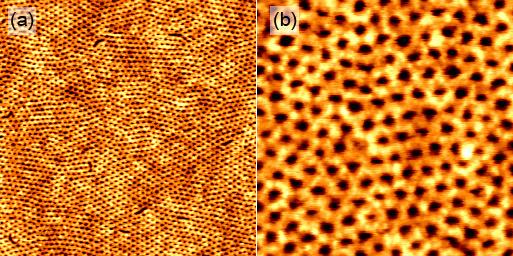
Figure 1. AFM images of copolymer template made from PS-b-PMMA. The voids (black features) are the washed PMMA which formed cylinder. The scan size is (a) 2 μm and (b) 0.5 μm, respectively. The holes are 20 nm (± 2nm) in diameter, and are around 40 nm (±1 nm) from one another.
Templates from Anodic Aluminum Oxide
A second method for producing a template is using anodic aluminum oxide membrane. When voltage is applied to an aluminum surface in oxalic acid, the aluminum surface is anodized in hexagonal pillar shape. The oxide layer is lifted off by applying HgCl solution and NaOH solution sequentially, and observed with AFM after being put down on silicon substrates. Figure 2 shows the AFM image of the membrane.
Measurement
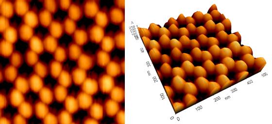
Figure 2. AFM images of anodic aluminum oxide membrane whose shape is hexagonal. The scan size is (a) 500 nm, and (b) is the 3D rendered image. The holes of cylinder are 50 nm (±2 nm) in diameter, and are around 100 nm (±5 nm) from one another.
It is crucial to control the size and the shape of the templates for the nanodot array applications. The dimension and the form of the units comprising the array are the key parameters which determine the properties of the array. Therefore, measuring and analyzing the status– size, shape, height, and distribution – of the templates and the produced nanodot array enables to control the production parameters. For the measurement and analysis, Scanning Electron Microscope (SEM) is used conventionally, which normally needs gold coating on the sample surface, which destructively affects the sample. On the contrary, AFM measures the sample without giving any deformation, and provides finer, more detailed data than what is provided by SEM. Park AFM which utilizes True Non-Contact mode for measurement, provides superior depth data which is one of the most crucial parameter of the nanodot array. Park AFM’s perfectly decoupled XY and Z-scanner enables the fast Z-scanner feedback which gives accurate height data and the symmetrical XY movement of the flexure guided XY-scanner which secures the linearity of the scanning.
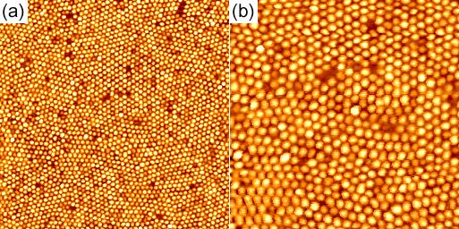
Figure 3. AFM images of Co/Pt nanodot array. The image shows that the array is arranged in hexagonal pattern locally. The scan sizes are (a) 2 μm and (b) 1 μm, respectively. The dots are 18 nm (±2 nm) in diameter, and are around 45 nm from one another.
Figure 3 shows the AFM images of Co/Pt film deposited on the PS copolymer template by pulsed laser deposition (PLD) method. Co/Pt target is ablated by the laser and fills the voids of the PS copolymer template. By measuring the template and so produced Co/Pt nanodot array, the optimal parameter for the template and PLD can be acquired. In Figure 3, the acquired AFM images show that the diameter and the distance between dots are 18 nm and 45 nm, respectively, which correspond to those of PS copolymer template.
References
1. F. S. Bates et. al., Annu. Rev. Phys. Chem. 41, 525 (1990).
2. G. M. Whiteside et. al, Science 254, 1312 (1991).
Acknowledgement
This note is based on the article, Journal of the Korean Vacuum Society 15, 427 (2006).
Samples and Images courtesy of Prof. Jeong Sook Ha, Korea University.


