


Electrical Property (EFM/KPFM)
The material and electrical properties of Zinc Oxide (ZnO) have made the compound attractive in the area of thin film transistors and light emitting diodes. Due to it non-toxic, wide bandgap and electrical conductivity, it is thought to be ideal for use in solar cell devices.
Publication on ZnO Using KPFM and the Park AFM
DR Doutt C Zgrabik, HL Mosbacker, LJ Brillson; Impact of near-surface native point defects, chemical reactions, and surface morphology on ZnO interfaces; J. Vac. Sci. Technol. B 26,4, Jul/Aug 2008 1477
Equipment: Park Systems XE-70
Abstract: The authors used a complement of depth-resolved cathodoluminescence spectroscopy _DRCLS_, atomic force microscopy _AFM_, and Kelvin probe force microscopy _KPFM_ to correlate the formation of native point defects with interface chemical reactions as well as surface morphology. A wide array of ZnO crystals grown by both melt and hydrothermal growth methods display orders-of-magnitude variation in 2.1, 2.5, and 3.0 eV native point defect optical transitions at their free surface and as a function of depth on a nanometer scale. AFM surface morphology scans taken simultaneously with KPFM potential maps reveal large variations in surface morphology related to the growth method and subsequent processing. Notably, when DRCLS defect emissions are low, the surface roughness is low and the morphology matches its respective KPFM potential map. When DRCLS emissions vary with depth, the morphology and potential maps do not correlate. Indeed, the latter can vary by hundreds of meV across micron square areas. These subsurface electrical changes are consistent with DRCLS features and emphasize the contribution of surface morphology to electrically active interface defects. The relative strength of near band edge to deep level defect emissions exhibit a threshold dependence on surface roughness.
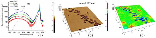
FIG. 3. _a_ DRCLS spectra for hydrothermally grown single crystal ZnO substrate MTI 15 alongside its respective _b_ AFM topography and _c_ KPFM potential map. DRCLS spectra show some of the highest bulk and surface NBE intensities and deep levels at 2.1 and 2.4 eV. The dashed curves represent the Gaussian deconvolution. Its KPFM potential map shows large _hundreds of mV_ potential changes across its surface.


