


General Considerations
Zinc Oxide (ZnO) – a wide bandgap (3.4 eV) II-VI compound semiconductor with a stable wurtzite structure (a=0.325 nm, c=0.521 nm) – offers tremendous potential for electronic, optoelectronic, and magnetoelectronic device applications. To date, it has attracted intensive research efforts for its unique properties and versatile applications in transparent electronics, ultraviolet light emitters, piezoelectric devices, chemical sensors and spin electronics. Based on its remarkable physical properties and the motivation of device miniaturization, large efforts have been focused on the synthesis, characterization, and device applications of ZnO nanomaterials. As such, an assortment of ZnO nanostructures, such as nanowires, nanotubes, nanorings, and nano-tetrapods have been successfully grown by a variety of methods, including chemical vapor deposition, thermal evaporation, electrodeposition, etc. These structures have been subjected to electrical transport, UV emission, gas sensing, and ferromagnetic doping studies, and considerable progress has been achieved.
The application prospects of ZnO nanostructures largely rely on the ability to control their location, alignment and packing density. Vertically aligned nanowires/nanorods have promising applications for electron field emitter, vertical transistor, and light emitting diodes (LEDs), thus have attracted enormous attention. Although the vertical alignment of ZnO nanostructures can be assisted by an electric field, for most cases, the alignment is realized by lattice matching between ZnO and the substrate utilized. Several types of epitaxial substrates have been utilized, including sapphire, GaN, ZnO film coated substrates, SiC, and Si. Although sapphire has been widely used as the epitaxy substrate for vertical growth of ZnO nanowires, it can be seen that GaN could be an even better candidate since it has a similar crystal structure and lattice constants to ZnO. Nanowires grown on GaN epilayers showed better vertical alignment than those produced on sapphire. The additional advantage of employing GaN as a substrate material instead of sapphire (and/or ZnO-based) rests in the fact that GaN has much better electrical properties and it is much easier to be doped with dopants to achieve p-type material.
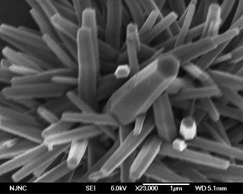
Figure 1. Hexagonally grown ZnO nanorod.
Direct measurements of the mechanical, piezoelectrical, optical, and magnetic properties of individual nanostructues are rather challenging since the traditional measurement methods used for bulk material do not apply. Typically, transmission electron microscopy (TEM) and scanning electron microscopy (SEM) have been employed to observe and measure physical dimensions and orientation of nanorods/nanowires. However, these conventional methods exhibit major limitations. Among these are spatial resolutions, sample preparation techniques, amount of time spent to collect data and so on. In addition, besides information on size and orientation no other physical properties characteristics may be investigated by both the TEM and SEM methods. On the other hand, atomic force microscopy (AFM) offers a simple, efficient, and non-destructive alternative to not only investigating mechanical properties (size, orientation, elastic properties, etc.) but also electric and magnetic characteristics of ZnO nano-structures.
Traditional AFM tools have been designed with the core of the scanning mechanism relying on an XYZ piezoelectric tube scanner. As such, cross-talk and non-linearity were inherently built in this design. The Park AFM scan system, which has been developed by Park Systems decoupled the XY and Z-scanners and was introduced as the next generation AFM design. As a result, the True Non-Contact mode was enabled.
Park AFM System Overview
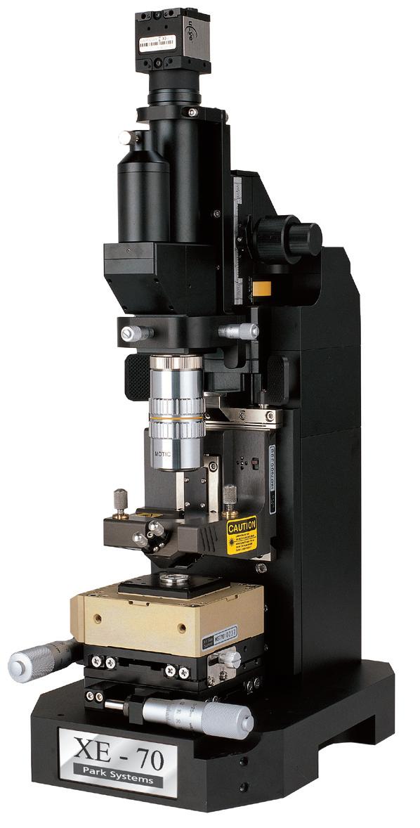
Figure 2. Based on Park AFM Scanning Technology, Park AFMs provide various SPM modes with outstanding stability and applicability.
The Park AFM scan system is a core feature that gives the competitive edge to the Park AFMs. Park Systems’ innovative scanner design separates the Z-scanner from the XY-scanner, enabling exceptional Z-servo performance, orthogonality, and scan accuracy.
The Z-scanner, which controls the vertical movement of the AFM tip and is fundamental to acquiring the surface morphology information, is completely decoupled from the XY-scanner which moves a sample in X and Y horizontal directions. From the structure, Park AFMs remove background curvature from a fundamental standpoint, and effectively eliminates the cross-talk and non-linearity problems that are intrinsic to conventional piezoelectric tube based AFM systems.
The Z-scanner is designed to have a higher resonant frequency than conventional piezoelectric tube scanners. For this reason, a stacked piezoelectric actuator is used for the Z-scanner with a high push-pull force when appropriately pre-loaded. Since the Z‑servo response of the Park AFM scan system is very accurate, the probe can precisely follow the steep curvature of a sample without crashing or sticking to the surface.
In the Park AFM scan system, the XY-scanner is a Body Guided Flexure scanner, which is used to scan a sample in the X and Y directions only. The flexure hinge structure of the XY-scanner guarantees highly orthogonal 2D movement with minimum out-of-plane motion. The 2D flexure stage of the Park AFM scan system has only 1-2 nm of out-of-plane motion for the scan range of 50 μm, compared to the inherent 80 nm by the piezoelectric tube scanner of conventional AFMs over the same scan range. (See “Technology behind the Park AFM” for detail.)
The symmetrical flexure scanner design also makes possible to place much larger samples on the sample stage than could normally be accommodated by a piezoelectric tube type scanner. Furthermore, the symmetry enables to keep the scanner balanced even when a sample is loaded, so that the dynamics of the XY-scanner is not distorted by the sample holder and/or the loaded sample. Since the flexure scanner only moves in the XY-direction, it can be scanned at much higher rates (10 Hz ~ 50 Hz) than would be possible with a standard AFM.
The Park AFM not only achieves a structural design innovation that yields a trend setting AFM performance, but it also brings state-of-the-art improvements to the electronics. The Park AFM Control Electronics incorporates advanced digital circuitry with precision software and hardware components that empower high speed and high capacity data processing, which are designed to enable the scanner, the core unit of the AFM, to provide efficient, accurate and fast control, and to facilitate the acquisition of stable images even beyond a scan speed of 10 Hz.
Besides the high speed measurement ability, Park AFM’s electronics controls the movement of the AFM system precisely by the closed-loop scan system, which is indispensable to map each additional property to the very point of enhanced topographic details. Even though an AFM system can acquire data with multiple modes, unless the system displays the exact position of measurement, it needs software correction (or calibration) to map the data on the exact position. Correction by software remapping usually works well when the imaging area is comparatively small, but closed-loop scan is applicable on any imaging area without distortion.
General Investigation of ZnO Nanorod Samples
Shown in Figures 2 are True Non-Contact AFM surface topography images at the 5 μm x 5 μm scale of ZnO nanorod samples grown on GaN-like substrates. For the GaN growth, sapphire was the substrate of choice. These ZnO nanorod specimens were grown by placing the GaN template in a solution of zinc nitrate and hexamethyl-tetramine held at a temperature of 60 °C. Both vertically and horizontally oriented nanorods are observed. Figure 3 (a) displays a three dimensional (3D) view of the scan area, while Figure 3 (b) shows both the top image view and line profile analysis results. Based on the data of Figure 3 (b), the typical height for the vertically oriented specimens is in the 0.3 nm to 0.6 nm range, while for the horizontal case, the length is in the 1.1 μm to 2.0 μm range with diameters up to 1.2 μm.
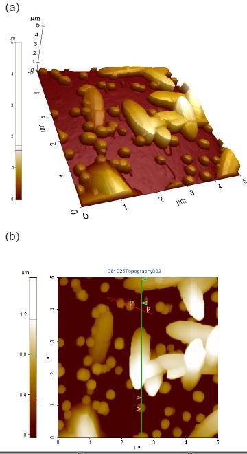
Figure 3. Surface morphology at the 5 μm × 5 μm scale of ZnO nanorod samples grown on GaN templates (a) 3D view and (b) top view with line analysis information. The image was acquired using high aspect ratio tip probes at 0.15 Hz with 256 x 256 pixel resolution.
Figures 3 are scanning electron microscopy (SEM) images (courtesy of Bell Labs, Lucent Technologies) of the same specimen as shown in Figures 2. The image magnifications are 15,000× for Figure 4 (a) and 30,000× for Figure 4 (b), respectively. For better imaging, a 45 degrees sample tilt angle was employed. Similar to the AFM imaging case, both horizontally and vertically oriented ZnO nanorods are observed with dimensions in the 0.30 nm to 0.50 nm height (vertical orientation), 1-2 μm length (horizontal orientation), and up to 1 μm diameter (horizontal orientation). Considering the fact that SEM imaging is performed at a 45 degree sample tilt angle, the physical nanorod dimensions based on the SEM evaluation are a very close match to the exact sizes directly observed by AFM investigation and shown in Figures 2.
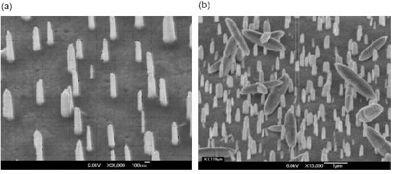
Figure 4. Scanning Electron Microscopy (SEM) images of the ZnO nanorod sample shown in Figures 3 (courtesy of Bell Labs, Lucent Technologies). Image magnification is 15,000x for figure (a) and 30,000x for figure (b), respectively. A 45 degrees sample tilt was employed.
Conclusion
One-dimensional (1D) semiconductor nanostructures, such as rods, wires, belts, and tubes have attracted much attention in recent years due to their unique properties and possibility to utilize them as building blocks for electronic, photonic, and life-science applications. ZnO is a direct-bandgap semiconductor with a large exciton binding energy, exhibiting near ultraviolet emission and piezoelectricity, bio-safe and biocompatible. Intensive research has been focused on fabricating one-dimensional ZnO nanostructures and in correlating their morphologies with their size-related optical, electrical, and magnetic properties. Among the 1D nanostructures, ZnO nanorods/nanowires have been widely studied because of their easy formation and device applications. AFM offers a direct, non-destructive, and easy to operate characterization method, which not only allows for exact mechanical properties measurements of ZnO nanostructures, but also provides means to enhancing the physical properties investigation by utilizing advanced scanning probe modes. The Park AFM instruments manufactured and distributed by Park Systems are equipped with state-of-the-art capabilities both in terms of standard (i.e., mechanical) and advanced (i.e., electrical, magnetic) options. The newest architectural design of the Park AFM tools comprising of decoupling of XY and Z-scanners and achievement of True Non-Contact scanning, enables these instruments with a wide range of scan parameters and scope of applications therein.
Note
Park Systems would like to thank Dr. Hock Ng of Bell Labs, Lucent Technologies for providing the ZnO nanorod samples and his technical contribution to preparing this document.
References
1. Z. Fan and J.G. Lu, article in press.
2. S.Y. Lee, E.S. Shim, H.S. Kang, S.S. Pang, and J.S. Kang, Thin Solid Films 437, 31 (2005).
3. S.J. Pearton, W.H. Heo, M. Ivill, D.P. Norton, and T. Steiner, Semicond. Sci. Technol. 19, R59 (2004).
4. S. Fujita, S.W. Kim, M. Ueda, and S. Fujita, J. Cryst. Growth 272, 138 (2004).
5. H. Zhou, and Z. Li, Mater. Chem. Phys. 89, 326 (2005).
6. D.W. Zeng, C.S. Xie, M. Dong, R. Jiang, X. Chen, A.H. Wang, J.B. Wang, and J. Shi, and A. Krost, Supperlatice Microst. 36, 95 (2004).
7. Z. Fan and J.G. Lu, article in press.
8. H.J. Fan, F. Fleischer, W. Lee, K. Nielsch, R. Scholz, M. Zacharias, U. Gosele, A. Dadgar, Appl. Phys. Lett. A79, 1865 (2004).


