


Christina Newcomb, Cathy Lee, Gerald Pascual, Byong Kim, and Keibock Lee
Park Systems Inc., Santa Clara, CA USA
The coupling between an electrical and mechanical response in a material is a fundamental property that provides functionality to a variety of applications ranging from sensors and actuators to energy harvesting and biology. Most materials exhibit electromechanical coupling in nanometer-sized domains. Therefore, to understand the relationship between structure and function of these materials, characterization on the nanoscale is required. This property can be directly measured in a non-destructive manner using piezoelectric force microscopy (PFM), a mode that comes standard in all atomic force microscopes (AFMs) from Park Systems. Additionally, PFM can be used as a spectroscopic tool to evaluate switching of piezoelectric domains. Here we demonstrate the utility of PFM for failure analysis of a multilayered ceramic capacitor. Correlative imaging of topography and electrical signals revealed discontinuous structures in the device that likely had a direct effect on device performance. Spectroscopy was also performed at a specific piezoelectric region to measure domain properties, such as the electric field required to flip the polarization direction (coercive voltage).
Introduction
From renewable energy to electronics and biology, there are variety of materials that exhibit a coupling of electrical and mechanical behavior. This coupling, known as a piezoelectric effect, is an intrinsic material property where the application of an electrical field induces a mechanical response. This material property is implemented in a multitude of applications ranging from ultrasonic imaging, to actuators and sensors.1 Common man-made piezoelectric materials include ceramics such as barium titanate and lead zirconate titanate while polymers such as polyvinylidene fluoride also exhibit piezoelectric properties. Naturally occuring piezoelectric materials include bone, quartz, and DNA.
Piezoelectric force microscopy (also referred to as piezoresponse force microscopy) is one of the most established non-destructive techniques to observe local electromechanical response at the nanometer length scale. Piezoelectric force microscopy, also termed dynamic-contact electrostatic force microscopy (DC-EFM) by Park, is performed in an atomic force microscope (AFM) operating in contact mode with an electrically-biased conductive tip to probe local nanoscale displacements in response to electronic stimuli. These sample displacements are often very small with a low signal-to-noise ratio; therefore, a lock-in amplifier is connected to the deflection signal to selectively drive the desired frequency and by-pass unwanted signal. Since the atomic force microscope’s photodiode is position-sensitive, piezoelectric force microscopy can also identify the direction of electrical polarization in active piezoelectric or ferroelectric domains. To capture this directionality, there are two distinct imaging modes: vertical piezoelectric force microscopy and lateral piezoelectric force microscopy (VPFM, LPFM) which are sensitive to domains polarized out-of-plane and in-plane, respectively.2 (Fig. 1) Taking both vertical and lateral components into account, one can identify the components of a local polarization vector to define the direction of the polarization vector using vector piezoelectric force microscopy.
Vertical Piezoelectric Force Microscopy | In VPFM, the cantilever will deflect normal to the sample surface in response to the applied bias, which indicates the presence of piezoelectric domains that point out-of-plane or normal to the sample surface (Fig. 1a-b). As a result, the EFM phase signal in the AFM will for example, appear bright for domains that point upward and dark for domains that point downward.
Lateral Piezoelectric Force Microscopy | In LPFM, to detect the piezoelectric domains that are pointed in-plane, the sample would exhibit a displacement shearing the surface. This lateral movement would result in a torsional displacement of the cantilever and would be detected by the position sensitive photodiode as a lateral deflection indicating a polarization direction parallel to the sample surface (Fig. 1c-d).
Vector Piezoelectric Force Microscopy | In piezoelectric samples with arbitrary crystallographic orientations, the application of a tip bias will result in both in-plane and out-of-plane displacements. By simultaneously collecting both vertical and lateral piezoelectric force microscopy signals, vector PFM can be performed to determine the final direction of the polarization vector in nanometer-sized grains. While piezoelectric constants of the material or a local orientation map can be obtained, most researchers assume that the local polarization orientation correlates with crystal orientation on the macroscale.3
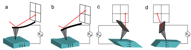
Figure 1 | A schematic representation of (a-b) vertical and (c-d) lateral PFM. The AFM laser shows vertical deflections which correspond with (a) downward or (b) upward out-of-plane electrical polarization. In lateral PFM, the cantilever will exhibit torsion in response to (c-d) lateral in-plane polarization directions. Black arrows indicate the direction of polarization vector in each case assuming that the relationship between polarization and crystal orientation is conserved.
It is also worthwhile to note that in a practical setting there are some limitations in combining vertical and lateral signals, as crosstalk can arise from geometrical constraints of the cantilever. Additionally, tip displacement in the lateral direction can be underestimated compared to surface displacement of the sample due to effects such as friction.4
Multilayer Ceramic Capacitors
Since piezoelectric materials have both sensing and actuating properties, they have countless applications in electronics industry.5 In particular, ceramics such as barium titanate exhibit piezoelectric behavior and have proven to be robust dielectric materials in capacitors, as they are cost effective and exhibit high intrinsic dielectric constants along with resistance to humidity and temperature. Multilayer ceramic capacitors (MLCC) are produced in large quantities, with over a trillion (1012) barium titanate-based MLCCs manufactured each year.6 They can be found in applications ranging from controlling the anti-lock brake system on a car to a heart monitor in a hospital. Society relies heavily on multilayer ceramic capacitors to be dependable, however they can susceptible to failure. For example, high temperatures from soldering or storage can cause thermal stress, resulting in cracking, increased current or shorts. A high-energy surge can also prove to be catastrophic and cause high leakage currents or rupture of the device itself. However, several of the devices may not pass specification after completing processing through the assembly line. To understand how the device fails whether during use, storage, or assembly, piezoelectric force microscopy, or PFM, is a powerful technique to analyze the functionality of devices, including MLLCs.
Here we report the analysis of a MLCC cross section using LPFM. We identify the discrete metal-dielectric domains within the device and we can also resolve regions within the dielectric material that exhibit unique polarization directions. Additionally, discontinuities in the individual materials can be observed in both topography and electrical signals, and likely affect device performance.
Experimental
A cross section of a MLCC was analyzed using a Park NX20 AFM and the LPFM signal was acquired using a scan rate of 0.2 Hz. A conductive NANOSENSORSTM PointProbe® Plus-Electrostatic Force Microscopy (PPP-EFM) cantilever (nominal spring constant k = 2.8 N/m and resonant frequency f = 25 kHz) coated with PtIr5 on both the front and back sides and nominal radius of curvature of 25 nm was used. The AFM tip was biased with 2V AC with no additional external bias applied to the sample during imaging.
Results and Discussion
A multilayer ceramic capacitor is typically monolithic with alternating dielectric (ceramic) and metal (electrode) layers that extend to corresponding connecting terminals at either end of the device (Fig. 2a). In this work, we characterize the cross section of a MLCC (cross section direction illustrated by the blue “slice” in Fig. 2a). The topography signal from this sample (Fig.2b) shows alternating vertical structures that correlate to dielectric and electrode layers. These alternating structures also lose continuity from the top of the image to the bottom of the image and are noted in the images by red arrowheads. These discontinuities could be representative of a defect in the device. Additionally, faint diagonal striations can be observed that are likely due to sample preparation where mechanical polishing was performed.
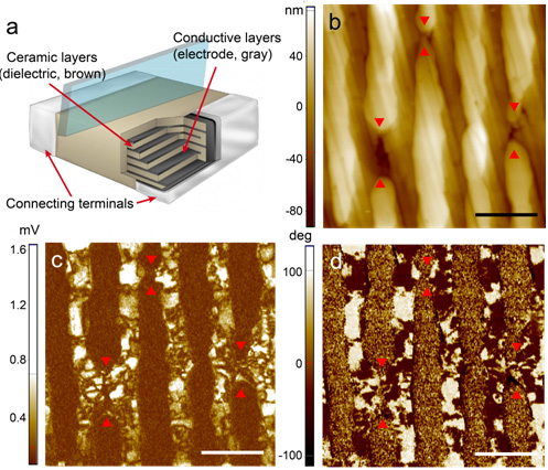
Figure 2 | The architecture and PFM results of the cross section of a MLCC. (a) A schematic of a MLCC device showing individual layers of the dielectric and electrode. The blue feature shows the plane that was cut to produce a cross section image show in panels b – d. (Image source: http://www.tonar.com/posts/kemet-news_3) The (b) topography (c) PFM amplitude and (d) PFM phase images of the cross section of a MLCC. Scalebars: 2 µm. Red arrowheads depict regions where the morphologies are discontinuous, suggesting device failure.
To further investigate the piezoelectric response of the device, representative lateral piezoelectric force microscopy amplitude and phase images were acquired. The PFM amplitude signal (Fig. 2c) defines the local electromechanical activity of the sample surface and directly follows sample displacement that results due to the piezoelectric effect. External contributions such as capacitive cantilever-surface interactions or electrostatic contributions can result in artifacts to the electromechanical signal and efforts to minimize this effect provide better quality data.3 The PFM phase signal (Fig. 2d) provides information about the polarization vector of the individual domains. Specifically, the piezo-response will oscillate in-phase or out-of-phase when the polarization direction is parallel or antiparallel to the field, respectively.
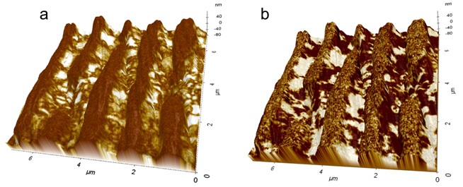
Figure 3 | 3D representation of MLCC (a) PFM amplitude and (b) PFM phase overlaid with height images showing discontinuities in the electrode and dielectric material traversing the electrodes at these defect sites.
The images acquired from the MLCC show regions that are taller in the topography image but lack amplitude or phase signals, suggesting that these regions do not exhibit piezoelectric behavior. Since the ceramic dielectric is known to be piezoelectric, this allows us to identify these non-responsive areas as regions containing the metal electrode. The dielectric layers also traverse the gaps in the electrode (Fig 2, red arrowheads and Fig. 3), which would contribute to reduced device performance and could potentially result in a failure to meet specification. Additionally, the amplitude and phase images of the MLCC show multiple domains within the piezoelectric material. The appearance of bright or dark regions indicate a difference in the direction of the polarization vector. The absolute direction of the vector (and meaning of bright and dark region in the phase image) will vary due to user setting such as the polarity of the applied bias. However, the domains that show a reversal in the phase signal (180º) as observed in Fig. 4, have opposite in-plane polarization directions (since LPFM is implemented here). Regions that show less than a 180º phase shift exhibit polarization directions that have both in-plane and out-of-plane components.
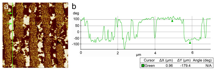
Figure 4 | LPFM phase represents the polarization direction of in-plane ferroelectric domains. (a) The image with a vertical line and (b) the corresponding line trace. The green arrows show the difference between light and dark regions which show a 180º phase shift. This shift demonstrates that these domains have parallel and antiparallel polarization directions.
PFM is also capable of performing spectroscopy at defined locations to measure the response to switching electric fields and sample hysteresis (also known as switching-spectroscopy PFM). The local ferroelectric behavior of the domains in the MLCC are characterized in Fig. 5. Theoretical curves demonstrating the relationship between strain and electric field (Fig. 5a) and the relationship between polarization and electrical field (Fig. 5d) are shown for reference.7,8 Since the amplitude directly measures displacement of the sample, the strain response as a function of sample bias can be measured in the dielectric of the MLCC (Fig. 5b, asterisk). Fig. 5c shows a characteristic "butterfly" shape that is similar to the ideal strain versus bias curve. The coercive voltage, which is a measure of ability to withstand an external electric field without depolarizing, is 0.7 V (See figure caption for details). The theoretical hysteresis loop of the phase (or polarization) response of a ferroelectric material is shown in Fig. 5d. The true response of the MLCC dielectric with sweeping electric field is shown in Fig. 5f demonstrates and sharp transition at the bias voltage of ~ 0.7 V. The offset of this value between sweeping from a negative to positive voltage and back demonstrates retention performance of the material. Repeated polarization reversal could also provide information about ferroelectric fatigue.
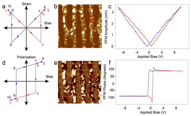
Figure 5 | PFM switching spectroscopy on the dielectric material of a MLCC. (a) The theoretical strain-bias response from a ferroelectric material. 1-5 depicts the behavior with increasing bias and 6-10 shows the response to reducing bias. Points 3 and 8 on this curve provide the coercive voltage for the material. (b) The PFM amplitude image and the (c) corresponding "butterfly" shape of the amplitude as the electric field was swept from -9V to +9 V (red) and back (blue). The red asterisk denotes the region that the spectroscopy was performed (d) The theoretical polarization-bias response from a ferroelectric material. 1-5 depicts the behavior with increasing bias and 6-10 shows the response to reducing bias. The distance between points 3 and 8 reflect retention performance of the material. (e) PFM phase image and (f) the corresponding phase behavior as the electric field was swept forward (red) and back (blue). The red asterisk denotes the location at which the spectroscopy was performed.
Conclusions
Here we demonstrate the use of lateral piezoelectric force microscopy to characterize the cross section of a MLCC. This technique enables nanoscale characterization of piezoelectric domains within the dielectric of the capacitor. The electrode was distinguished from the dielectric and discontinuities in the device were identified as regions that would be expected to compromise device performance. Both the response in strain (amplitude) and polarization (phase) as a function of applied bias were explored to evaluate material characteristics including hysteresis and coercive voltage. Overall, the ability to characterize the piezoresponse of materials at the nanoscale and quantify the polarization vector of a material with applied electric field enables researchers to perform local electric measurements and establish structure-property relationships for multiple applications.
References
1. Ikeda T. Piezoelectricity. Oxford university press; 1990.
2. Soergel E. Piezoresponse force microscopy (PFM). J Phys D Appl Phys. 2011;44(46):464003.
3. Kalinin S V., Rodriguez BJ, Jesse S, et al. Vector Piezoresponse Force Microscopy. Microsc Microanal. 2006;12(3):206. doi:10.1017/S1431927606060156.
4. Peter F, Rüdiger A, Waser R. Mechanical crosstalk between vertical and lateral piezoresponse force microscopy. Rev Sci Instrum. 2006;77(3):36103.
5. Vijaya MS. Piezoelectric Materials and Devices: Applications in Engineering and Medical Sciences. CRC Press; 2012.
6. Ho J, Jow TR, Boggs S. Historical introduction to capacitor technology. IEEE Electr Insul Mag. 2010;26(1):20-25. doi:10.1109/MEI.2010.5383924.
7. Bdikin IK, Kholkin AL, Morozovska AN, Svechnikov S V., Kim SH, Kalinin S V. Domain dynamics in piezoresponse force spectroscopy: Quantitative deconvolution and hysteresis loop fine structure. Appl Phys Lett. 2008;92(18). doi:10.1063/1.2919792.
8. Koval V, Viola G, Tan Y. Biasing effects in ferroic materials. Ferroelectr Mater Charact. 2015.


