


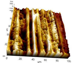
Figure 1. Non-Contact mode topography image of a stainless steel wafer measured using an XE-150. Automated step and scan measurements on the wafer revealed an average surface roughness of ~ 100 nm.
Roughness measured on the Park AFM is quick and easy from extreme roughness values over large scan areas to minute features for small scan areas. The power of the instrument for roughness measurements lies in its sub-angstrom noise floor, allowing measurements of the smoothest samples with accuracy, repeatability, and long tip lifetime.
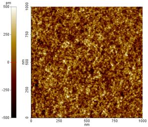
Figure 2. Non-Contact mode measurement of a hard drive disk media sample taken with the XE-HDM. The rms roughness measured for the sample was 1.55 A.
Park AFM Productivity in Action
Yong-Jin Seo, Nam-Hoon Kim, Eui-Goo Chang, Jinseong Park, Pil-Ju Ko and Woo-Sun Leea; Chemical mechanical planarization characteristics of WO3 thin film for gas sensing; J. Vac. Sci. Technol. A 23.4., Jul/Aug 2005 737
Equipment: Park Systems XE-200
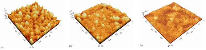
Abstract: It is important to control the microstructure and surface of films to use them in gas sensors. Chemical mechanical polishing sCMPd processing is one of the most useful methods for improving the surface roughness of films. The effects of CMP on the surface morphology of WO3 thin films prepared by the rf sputtering system were investigated in this article. The removal rate of the films increased, and the rms surface roughness decreased with the addition of an oxidizer to the tungsten slurry. Within-wafer nonuniformity was improved to below 5% when oxidizers of 5.0 and 2.5 vol %, respectively, were added to the tungsten slurry. The optimized oxidizer concentration, reflected by both the rms roughness values and a hillock-free surface with the good uniformity, was 5.0 vol % as shown with atomic force microscopy analysis of thin film topographies. Our CMP results will be a useful reference for advanced technology of thin films for gas sensor applications in the near future.
Samples:
- Stainless Steel
- Hard Drive Media
Image Conditions:
- True Non-Contact
- 1 Hz or less scan rates
System Requirement:
- High bandwidth Z-actuator
- Low-coherence otical diode
- Decoupled XY and Z scanners, 0.5A Noise Floor
The Benefits:
The high bandwidth Z- actuator enables imaging of smooth or rough surfaces without tip or sample damage. The low-coherence optical source prevents optical interference creating false waviness in an image. The decoupled Z scanner prevents artificial bow in the image. Therefore accurate roughness values for a variety of samples can be measured. Extrememly low roughness samples can be measured easily with the Park AFMs.


